Three-layer pixel structure of micro-bolometer

A microbolometer, pixel structure technology, applied in optical radiometry, electrical radiation detectors, radiation pyrometry, etc., can solve problems such as limiting device integration, affecting thermal sensitivity, and limiting device infrared absorptivity

Active Publication Date: 2021-09-14
HARBIN INST OF TECH
View PDF12 Cites 0 Cited by
  • Summary
  • Abstract
  • Description
  • Claims
  • Application Information

AI Technical Summary

Problems solved by technology

[0004] The traditional microbolometer is composed of a single-layer pixel structure, in which the infrared absorbing layer and the heat-sensitive layer are on the same bridge surface, which causes the temperature of the infrared absorbing layer and the heat-sensitive layer to change at the same time, and it is difficult to reduce the temperature of the pixel. Guide while increasing the absorption rate of infrared light, thereby limiting the thermal sensitivity of the pixel
If the infrared absorption of the single-layer pixel is increased, the area of ​​the bridge surface needs to be continuously increased, which also limits the integration of the device, so the single-layer structure cannot meet the high performance requirements of the device, and the development of the single-layer micro-bridge has limitations.
[0005] There are roughly two types of existing double-layer microbolometers, one is a double-layer S-shaped structure, which is divided into two independent bridge decks, the light-absorbing layer and the heat-sensitive laye...

Method used


Image

  • Three-layer pixel structure of micro-bolometer
  • Three-layer pixel structure of micro-bolometer
  • Three-layer pixel structure of micro-bolometer

Examples


specific Embodiment approach 1

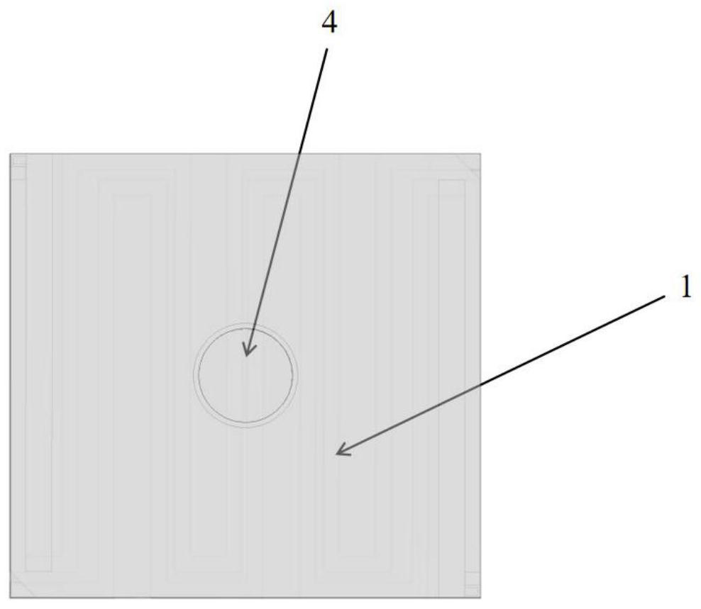
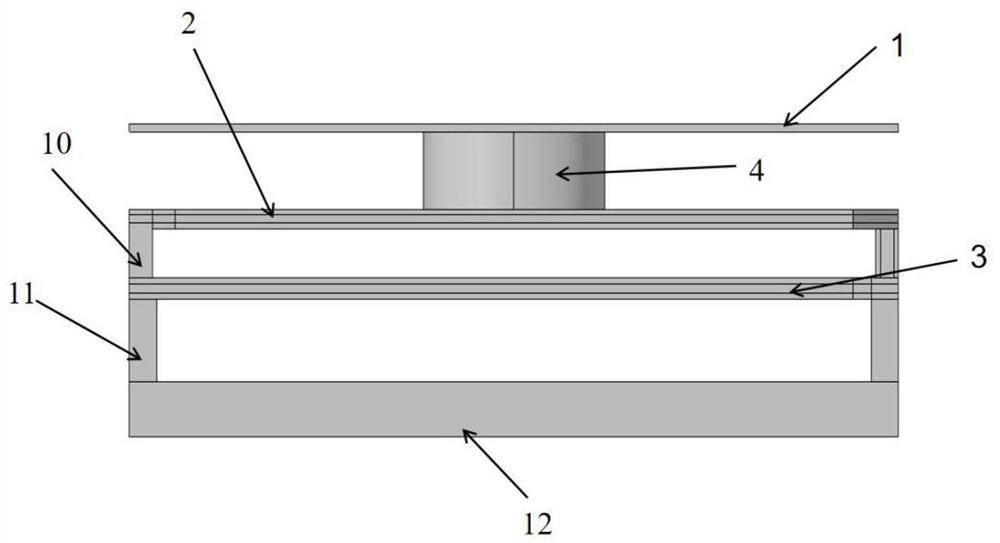
[0023] Specific Embodiment 1: This embodiment describes a three-layer pixel structure of a microbolometer. The three-layer pixel structure is a light-absorbing layer 1, a heat-sensitive layer 2, and an electrode layer from top to bottom. 3. The light-absorbing layer 1 and the heat-sensitive layer 2 are connected through hollow bridges 4, an optical resonant cavity is formed between the light-absorbing layer 1 and the heat-sensitive layer 2, and two electrodes 5 are embedded in the heat-sensitive layer 2, The two electrodes 5 are located on two opposite sides of the thermosensitive layer 2, and the electrode layer 3 includes an electrode layer bridge surface and two rows of bridge legs 6 in a centrally symmetrical triple folded detour structure that are not in contact with each other on the upper surface. and bridge leg two 7, the head end and tail end of each said triple folded circuitous structure are respectively provided with hole one 8 and hole two 9, and the two diagonal s...

specific Embodiment approach 2

[0024] Embodiment 2: In the three-layer pixel structure of a microbolometer described in Embodiment 1, the light-absorbing layer 1 has a thickness of 0.1um-0.2um and is located on the top of the microbridge. Make the light absorbing layer 1 equal to the pixel area. An optical resonant cavity is formed with the thermosensitive layer 2 . Debugging by the matlab program shows that when the thickness of the light absorbing layer 1 is 0.1um-0.2um, the infrared absorption rate can reach more than 90%.

specific Embodiment approach 3

[0025] Specific embodiment three: the three-layer pixel structure of a microbolometer described in specific embodiment one, the height of the hollow bridge column 4 is 2um-2.5um, the thickness is 0.2um-0.5um, and the radius is 2um-3um. The upper surface is a light absorbing layer 1 and the lower surface is a thermosensitive layer 2 . According to the theory of optical resonant cavity, the hollow bridge column 4 has the highest light absorption efficiency when the cavity height is λ / 4. Since the infrared light absorption rate of the pixel is the highest for 8um-10um, the selected height is 2um-2.5um. In consideration of its mechanical stability, the area of ​​the top and bottom of the cylinder should not be too low, and in consideration of the light absorbing layer 1 and the heat sensitive layer 2, the area of ​​the top and bottom of the cylinder should not be too high. Considering the reduction of heat capacity, the thickness of the side wall of the cylinder should not be too...


PUM

PropertyMeasurementUnit
Thicknessaaaaaaaaaa
Thicknessaaaaaaaaaa
Thicknessaaaaaaaaaa

Abstract

A three-layer pixel structure of a micro-bolometer comprises a light absorption layer, a thermosensitive layer, an electrode layer and a substrate of the electrode layer. An optical resonant cavity is formed between the light absorption layer and the thermosensitive layer which are connected through a hollow bridge column, so that the microbridge heat capacity is reduced. The thermosensitive layer maximizes the absorptivity of a thermistor layer to infrared transmission light, and the electrode layer bends and arranges electrode bridge legs from two ends, so that the length of the bridge legs is increased, and the thermal conductivity is reduced. Passivation layers are laid above and below the thermosensitive layer and the electrode layer, and the electrode bridge legs are connected with the thermistor layer and the substrate respectively to achieve electrical communication and thermal communication. While time response constants are considered, a high infrared absorption rate and low thermal conductivity are achieved, the temperature rise of pixels is effectively improved, and high temperature response rate and high thermal sensitivity are achieved.

Description

technical field [0001] The invention belongs to the technical field of uncooled infrared detectors, and in particular relates to a three-layer pixel structure of a microbolometer. Background technique [0002] With the development of infrared imaging technology, the application range of infrared imaging system is getting wider and wider, including communication, medical treatment, chemistry, biology, and war, and low-cost commercialization has been realized. In terms of system application, the thermal imaging system’s Important parameters such as time response constant, infrared absorptivity and thermal sensitivity (equivalent noise temperature difference) have become the focus of research. Among them, the uncooled heat detector has the advantages of no need for refrigeration, light weight, miniaturization, and convenient use. Uncooled infrared detectors are also developing toward large arrays and miniaturized pixel sizes, and have been widely used in military, medical, agr...

Claims


Application Information

Patent Timeline
IPC IPC(8): G01J5/00G01J5/24
CPCG01J5/0003G01J5/00G01J5/24G01J2005/0077
Inventor 冯睿安宁孙芳魁丁卫强曹永印
Owner HARBIN INST OF TECH
Why Eureka
Try Eureka