Manufacturing method of electromagnetic shielding material, electromagnetic shielding material and electronic product
A technology of electromagnetic shielding materials and manufacturing methods, which is applied in the fields of magnetic field/electric field shielding, metal material coating technology, electrical components, etc., and can solve the problems of affecting the performance of electromagnetic shielding films, reducing the thickness of electromagnetic shielding materials, and increasing the complexity of electromagnetic shielding films and other issues, to achieve the effect of improving the use effect and flexibility of use, reducing material costs, and overcoming poor plating
- Summary
- Abstract
- Description
- Claims
- Application Information
AI Technical Summary
Problems solved by technology
Method used
Image

Examples
Embodiment 1
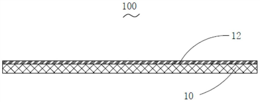
[0043] A polymer film layer is provided, the thickness of the polymer film layer is 1.5 microns, and the material is polyethylene terephthalate.
[0044] The polymer film layer is baked at a temperature of 45 degrees centigrade for 24 hours.
[0045] Corona treatment is performed on one surface of the baked polymer film layer, and the corona treatment time is 1 second. The surface had a dyne value of 50 after corona treatment.
[0046] A layer of metal shielding layer is sputtered on the roughened surface of the polymer film layer, using copper as the target material, and continuous winding coating is adopted. The coating process conditions are: vacuum degree 0.2Pa, continuous winding plating speed 15m / min, the coating current is 1A, and the coating voltage is 700V. The resulting metal shielding layer had a thickness of 3000 nm.
[0047] The metal shield is subjected to anti-oxidation treatment with a peroxygen protectant.
Embodiment 2
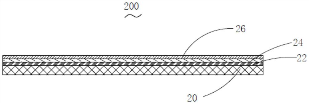
[0049] A polymer film layer is provided, the thickness of the polymer film layer is 4 microns, and the material is polycarbonate.
[0050] The polymer film layer is baked at a temperature of 80 degrees centigrade for 1 hour.
[0051] Corona treatment is performed on one surface of the baked polymer film layer, and the corona treatment time is 10 seconds. The surface had a dyne value of 56 after corona treatment.
[0052] The first layer of metal shielding layer is sputtered on the roughened surface of the polymer film layer, using zinc as the target material, and continuous winding coating is adopted. The coating process conditions are: vacuum degree 0.02Pa, continuous winding coating speed is 30m / min, the coating current is 30A, and the coating voltage is 680V. The obtained first metal shielding layer had a thickness of 1000 nanometers.
[0053] The second metal shielding layer is sputtered on the surface of the first metal shielding layer, with copper as the target mater...
Embodiment 3
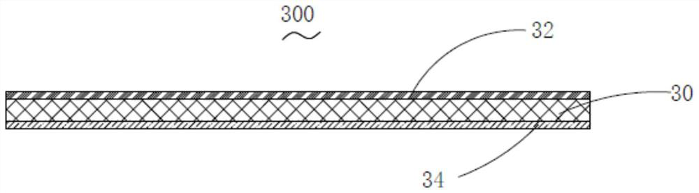
[0055] A polymer film layer is provided, the thickness of the polymer film layer is 2 microns, and the material is polypropylene.
[0056] The two surfaces of the polymer film layer were subjected to corona treatment, and the corona treatment time was 5 seconds respectively. The dyne values of the two surfaces after corona treatment were 40 respectively.
[0057] A layer of metal shielding layer is respectively sputtered on the two surfaces of the roughened polymer film layer, with titanium as the target material, and continuous winding coating is adopted. The coating process conditions are: vacuum degree 0.2Pa, continuous winding coating speed It is 295m / min, the coating current is 1A, and the coating voltage is 700V. The thickness of each metal shielding layer obtained is 3000 nanometers; or the thickness of one metal shielding layer is 1500 nanometers, and the thickness of the other metal shielding layer is 3000 nanometers.
PUM
| Property | Measurement | Unit |
|---|---|---|
| Thickness | aaaaa | aaaaa |
| Thickness | aaaaa | aaaaa |
| Thickness | aaaaa | aaaaa |
Abstract
Description
Claims
Application Information
 - R&D
- Intellectual Property
- Life Sciences
- Materials
- Tech Scout
- Unparalleled Data Quality
- Higher Quality Content
- 60% Fewer Hallucinations
Browse by: Latest US Patents, China's latest patents, Technical Efficacy Thesaurus, Application Domain, Technology Topic, Popular Technical Reports.
© 2025 PatSnap. All rights reserved.Legal|Privacy policy|Modern Slavery Act Transparency Statement|Sitemap|About US| Contact US: help@patsnap.com