Negative-electrode active material and method for producing same
A negative electrode active material and simple substance technology, applied in the field of negative electrode active material and its preparation, can solve the problems of electrolyte consumption and battery cycle characteristics degradation, and achieve the effects of high initial efficiency, stable slurry, and good initial charge and discharge characteristics
- Summary
- Abstract
- Description
- Claims
- Application Information
AI Technical Summary
Problems solved by technology
Method used
Image
Examples
Embodiment 1-1
[0193] First, a negative electrode active material was prepared in the following manner. The raw material mixed with metal silicon and silicon dioxide is introduced into the reaction furnace, and the material formed by vaporizing it in an atmosphere with a vacuum degree of 10Pa is deposited on the adsorption plate and cooled sufficiently, then the deposit is taken out and pulverized by a ball mill . SiO of silicon compound particles obtained in this way x has an x-value of 1.0. Next, the particle diameter of the silicon compound particles is adjusted by classification. Then, by performing pyrolytic CVD, the carbon material is coated on the surface of the silicon compound particles.
[0194] Next, the silicon compound particles are modified by absorbing lithium by a redox method. Then, heating is performed in the range of 450°C to 750°C to perform modification.
[0195] The particle size of the obtained negative electrode active material particles and the thickness of the ...
Embodiment 1-2、1-3
[0205] The negative electrode active material was prepared in the same manner as in Example 1-1 except that the heat treatment temperature and treatment atmosphere conditions were changed. In addition, each measurement was performed in the same manner as in Example 1-1.
Embodiment 2-1~ Embodiment 2-4
[0217] In addition, the preparation of the negative electrode active material was performed in the same manner as in Example 1-1, except that the crystallinity of silicon was controlled by changing the bath temperature at the time of lithium doping and the subsequent heat treatment conditions. In addition, each measurement was performed in the same manner as in Example 1-1.
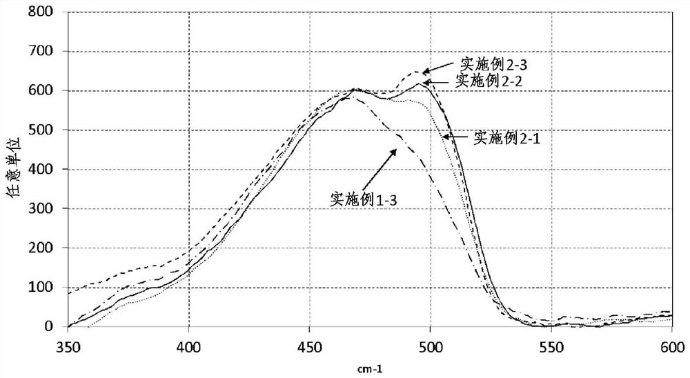
[0218] Table 2 shows the evaluation results of Example 2-1 to Example 2-4. In addition, the Raman spectra obtained by the negative electrode active materials of Examples 1-3, 2-1 to 2-3 are shown in image 3 , the Raman spectrum obtained by the negative electrode active material of Example 2-4 is shown in Figure 4 .
[0219] [Table 2]
[0220]
[0221] As shown in Table 2, the higher the crystallinity of silicon, the faster gas is generated. Considering the manufacturing process of the lithium ion secondary battery, the peak of crystalline silicon is less than 1.1A≧B (Example 2-3), which enables m...
PUM
| Property | Measurement | Unit |
|---|---|---|
| particle size | aaaaa | aaaaa |
| thickness | aaaaa | aaaaa |
| particle diameter | aaaaa | aaaaa |
Abstract
Description
Claims
Application Information
 - R&D
- Intellectual Property
- Life Sciences
- Materials
- Tech Scout
- Unparalleled Data Quality
- Higher Quality Content
- 60% Fewer Hallucinations
Browse by: Latest US Patents, China's latest patents, Technical Efficacy Thesaurus, Application Domain, Technology Topic, Popular Technical Reports.
© 2025 PatSnap. All rights reserved.Legal|Privacy policy|Modern Slavery Act Transparency Statement|Sitemap|About US| Contact US: help@patsnap.com


