
Preparation method of enhanced photoelectric detector substrate, product thereof and enhanced III-V photoelectric detector

A photodetector, III-V technology, applied in the field of photodetectors, can solve the problems of high fabrication cost of III-V detectors, reduced performance of III-V devices, and inability to integrate circuits, so as to enhance light absorption efficiency and improve Signal-to-noise ratio, the effect of improving quality

Active Publication Date: 2021-07-02
SUZHOU INST OF NANO TECH & NANO BIONICS CHINESE ACEDEMY OF SCI
View PDF4 Cites 0 Cited by
  • Summary
  • Abstract
  • Description
  • Claims
  • Application Information

AI Technical Summary

Problems solved by technology

[0006] However, the high prices of substrates such as GaAs and InP make the preparation cost of corresponding III-V detectors relatively high, and substrates such as GaAs and InP Larger size, can not be integrated with the circuit
[0007]Si substrate can be used to make III-V detectors due to its mature preparation process, high crystal quality, and low price, but due to its There is a large lattice mismatch and thermal mismatch with III-V compounds, which will generate a large number of threading dislocations during the growth process, and there is a reverse domain boundary problem, which greatly reduces the performance of III-V devices

Method used


Image

  • Preparation method of enhanced photoelectric detector substrate, product thereof and enhanced III-V photoelectric detector
  • Preparation method of enhanced photoelectric detector substrate, product thereof and enhanced III-V photoelectric detector
  • Preparation method of enhanced photoelectric detector substrate, product thereof and enhanced III-V photoelectric detector

Examples


Embodiment Construction

[0035] Objects, advantages and features of the present invention will be illustrated and explained by the following non-limiting description of preferred embodiments. These embodiments are only typical examples of applying the technical solutions of the present invention, and all technical solutions formed by adopting equivalent replacements or equivalent transformations fall within the protection scope of the present invention.

[0036] In the description of the scheme, it should be noted that the terms "center", "upper", "lower", "left", "right", "front", "rear", "vertical", "horizontal", " The orientation or positional relationship indicated by "inner", "outer", etc. is based on the orientation or positional relationship shown in the drawings, and is only for the convenience of description and simplification of description, rather than indicating or implying that the device or element referred to must have a specific orientation , constructed and operated in a particular or...


PUM

PropertyMeasurementUnit
thicknessaaaaaaaaaa
thicknessaaaaaaaaaa
thicknessaaaaaaaaaa

Abstract

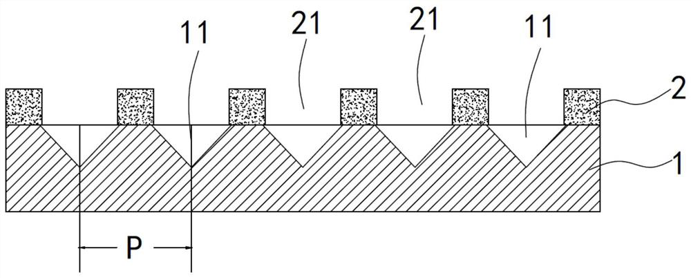
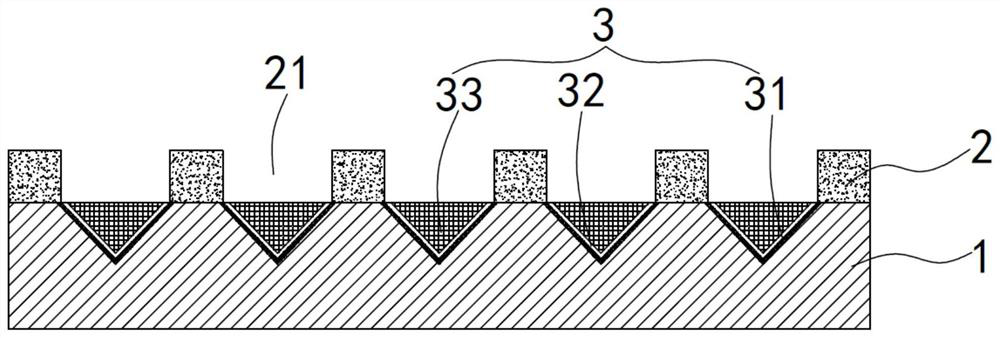
The invention discloses a preparation method of an enhanced photoelectric detector substrate, a product thereof and an enhanced III-V photoelectric detector. The method comprises the following steps: forming an inverted triangular groove with a specific period in a silicon (001) substrate through employing the anisotropy characteristic of a silicon (001) substrate material, and filling a III-V material seed layer, thereby obtaining a reflection-increasing structure. According to the scheme, light penetrating through the detector from the front side can be effectively reflected, the light passes through an active area of a device again, the purpose of enhancing the light absorption efficiency is achieved, and the effects of enhancing a detection signal and improving the signal-to-noise ratio are achieved. According to the scheme, the modulation effect of the grating on light waves with specific wavelengths and the application characteristics of silicon-based three-five integration are utilized, so the reverse domain boundary problem caused by direct lattice mismatch between the silicon crystal and the III-V material is effectively solved, favorable conditions are created for integration of the silicon (001) substrate and the III-V area array device, and the quality of the device is improved.

Description

technical field [0001] The invention relates to the field of photodetectors, in particular to a preparation method of an enhanced photodetector substrate, a product thereof and an enhanced III-V photodetector. Background technique [0002] III-V detectors have a wide range of applications in life, including infrared thermometers, thermal imagers, gas detectors, etc. At the same time, area array detectors and area array lasers have been successfully applied to life and aerospace. Obtain high-quality devices. [0003] The core sensing layer of the PN junction detector is a PN junction composed of P-type semiconductor and N-type semiconductor. Under the action of the electric field, a photocurrent is formed in the external circuit, thereby realizing the photodetection function. [0004] In conventional III-V detectors, light can only pass through the active region once, so the light absorption efficiency is relatively low, resulting in low signal strength and signal-to-noise ...

Claims


Application Information

Patent Timeline
Patent Type & Authority Applications(China)
IPC IPC(8): H01L31/18H01L31/0232H01L31/0236H01L31/0304
CPCH01L31/03042H01L31/02366H01L31/02327H01L31/1852Y02P70/50
Inventor 董旭熊敏张宝顺
Owner SUZHOU INST OF NANO TECH & NANO BIONICS CHINESE ACEDEMY OF SCI
Learn More