Electronic component packaging body, electronic component assembling structure and electronic equipment

A technology for electronic components and assembly structures, applied in the direction of electrical components, printed circuits connected by non-printed electrical components, electrical solid devices, etc., can solve the problems affecting the reliability of packaging components, poor reliability, and solder joint fractures

Active Publication Date: 2021-06-29
HUAWEI DIGITAL POWER TECH CO LTD
View PDF7 Cites 2 Cited by
  • Summary
  • Abstract
  • Description
  • Claims
  • Application Information

AI Technical Summary

Problems solved by technology

However, since the contact array package is a surface mount package, the package component and the circuit board are soldered through surface contact, the reliability of welding is poor, and it is easy to cause breakage at the solder joint, which affects the reliability of the package component

Method used


Image

  • Electronic component packaging body, electronic component assembling structure and electronic equipment
  • Electronic component packaging body, electronic component assembling structure and electronic equipment
  • Electronic component packaging body, electronic component assembling structure and electronic equipment

Examples


Embodiment Construction

[0063] Embodiments of the present application are described below with reference to the drawings in the embodiments of the present application.

[0064] The present application provides an electronic device. An electronic device includes a casing and an electronic component assembly structure. The electronic component assembly structure is installed on the casing. Electronic devices can be products such as mobile phones, tablets, laptops, in-vehicle devices, wearable devices, drones, and routers. The electronic device may also be a power supply module, a communication signal transmitting base station, a network switching device and the like. In this embodiment, description is made by taking the electronic device as an in-vehicle device as an example.

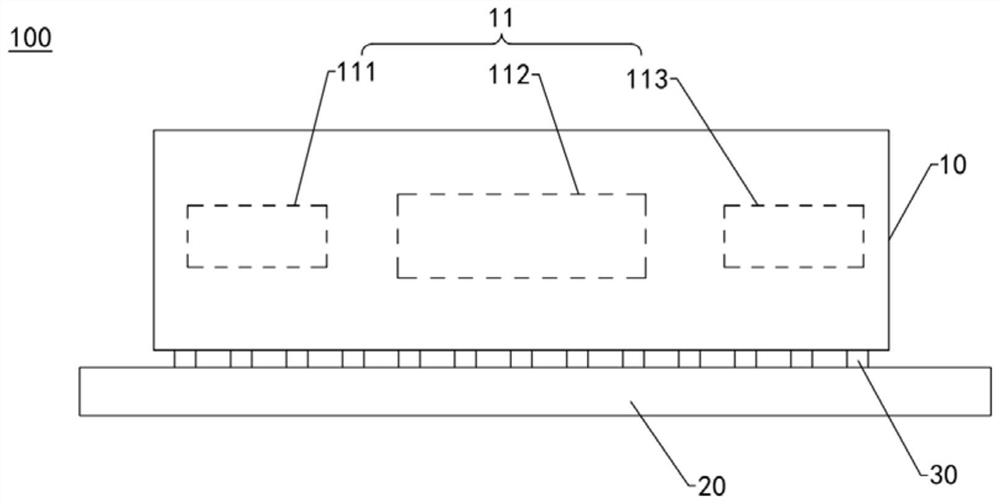
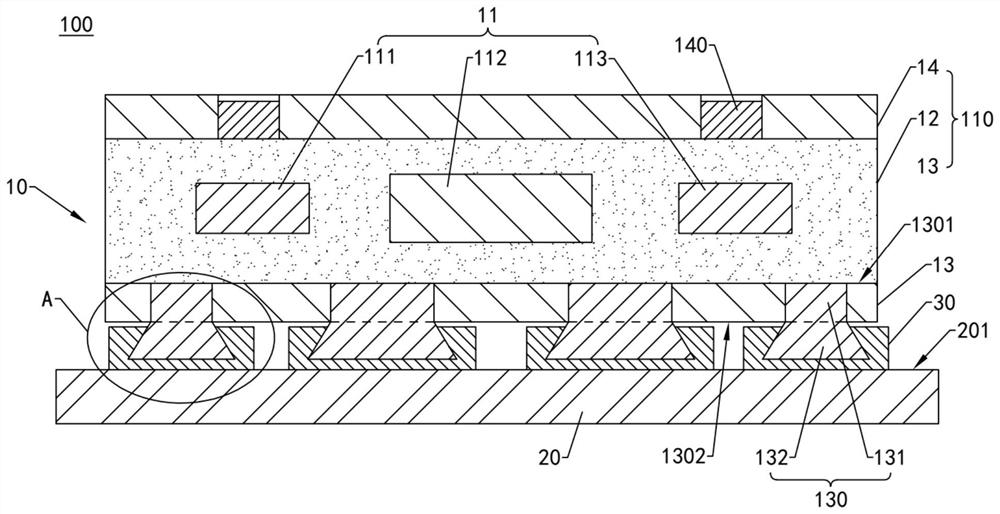
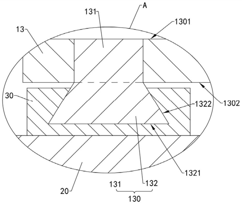
[0065] see figure 1 , figure 1 It is a partial structural schematic diagram of the electronic component assembly structure 100 provided by the embodiment of the present application. Such as figure 1 As shown, the elect...


PUM


Abstract

An embodiment of the invention discloses an electronic component packaging body, an electronic component assembling structure and electronic equipment. The electronic component assembling structure comprises the electronic component packaging body, a circuit board and welding spots, wherein the electronic component packaging body comprises a substrate, an electronic component and a pin, the electronic component is packaged in the substrate, the pin is electrically connected with the electronic component, the pin comprises a first part and a second part connected with the first part, the first part is embedded in the substrate, the second part protrudes relative to the substrate, the second part comprises a bottom surface and a side surface, the bottom surface is an outer surface, far away from the substrate, of the pin, and the side surface is connected between the bottom surface and the substrate; the electronic component packaging body is mounted on the circuit board, and the circuit board is electrically connected with the electronic component; and the welding spots are connected between the pins and the circuit board and surround the bottom surface and the side surfaces of the second part. According to the electronic component assembling structure provided by the invention, the welding reliability of the electronic component packaging body and the circuit board is relatively high.

Description

technical field [0001] The present application relates to the field of packaging technology, in particular to an electronic component packaging body, an electronic component assembly structure and electronic equipment. Background technique [0002] With the development of electronic products towards multi-functionality and portability, chip-embedded packaging has become a research hotspot in the field of electronic component packaging technology. The existing chip-embedded packaging substrate generally adopts a land grid array (LGA) package to realize the fixing between the package component and the circuit board. However, since the contact array package is a surface mount package, the package component and the circuit board are soldered through surface contact, the reliability of welding is poor, and it is easy to cause breakage at the solder joint, which affects the reliability of the package component. Contents of the invention [0003] The application provides an elec...

Claims


Application Information

Patent Timeline
Patent Type & Authority Applications(China)
IPC IPC(8): H05K1/18
CPCH05K1/182H05K1/185H01L23/49811H01L23/5389H01L2924/19105H01L2924/19041H01L2924/19043H01L2224/12105H01L2224/04105H01L2924/19107H01L24/20H01L23/552H01L2924/3025H01L23/3121H01L25/16H05K1/181H05K2201/10719
Inventor 向志强
Owner HUAWEI DIGITAL POWER TECH CO LTD
Why Eureka
Try Eureka