Large-size silicon wafer double-sided polishing method

A double-sided polishing and large-size technology, which is applied in the direction of surface polishing machine tools, grinding/polishing equipment, grinding machines, etc., can solve the problems of low polishing efficiency, poor consistency, and poor polishing effect, and achieve good cleaning effect and polishing Good effect and stable geometric parameters

Inactive Publication Date: 2021-06-22
TIANJIN ZHONGHUAN ADVANCED MATERIAL TECH +1
View PDF12 Cites 0 Cited by
  • Summary
  • Abstract
  • Description
  • Claims
  • Application Information

AI Technical Summary

Problems solved by technology

[0003] The invention provides a double-sided polishing method for large-size silicon wafers, which solves the technical problems of large-size silicon wafer flatness, poor consistency, poor polishing effect, and low polishing efficiency in the prior art.

Method used


Image

  • Large-size silicon wafer double-sided polishing method
  • Large-size silicon wafer double-sided polishing method
  • Large-size silicon wafer double-sided polishing method

Examples


Embodiment Construction

[0036] The present invention will be described in detail below in conjunction with the accompanying drawings and specific embodiments.

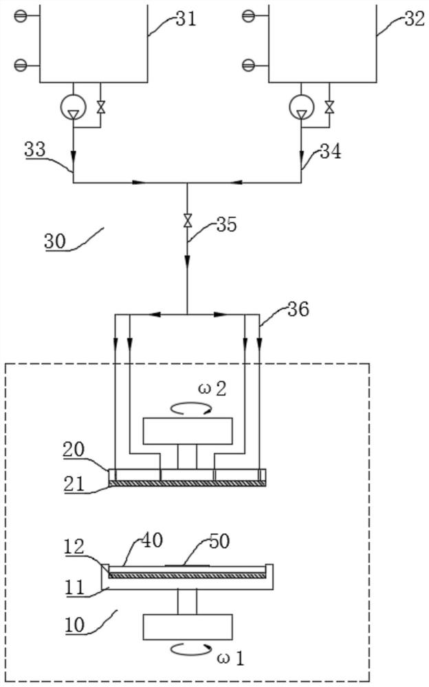
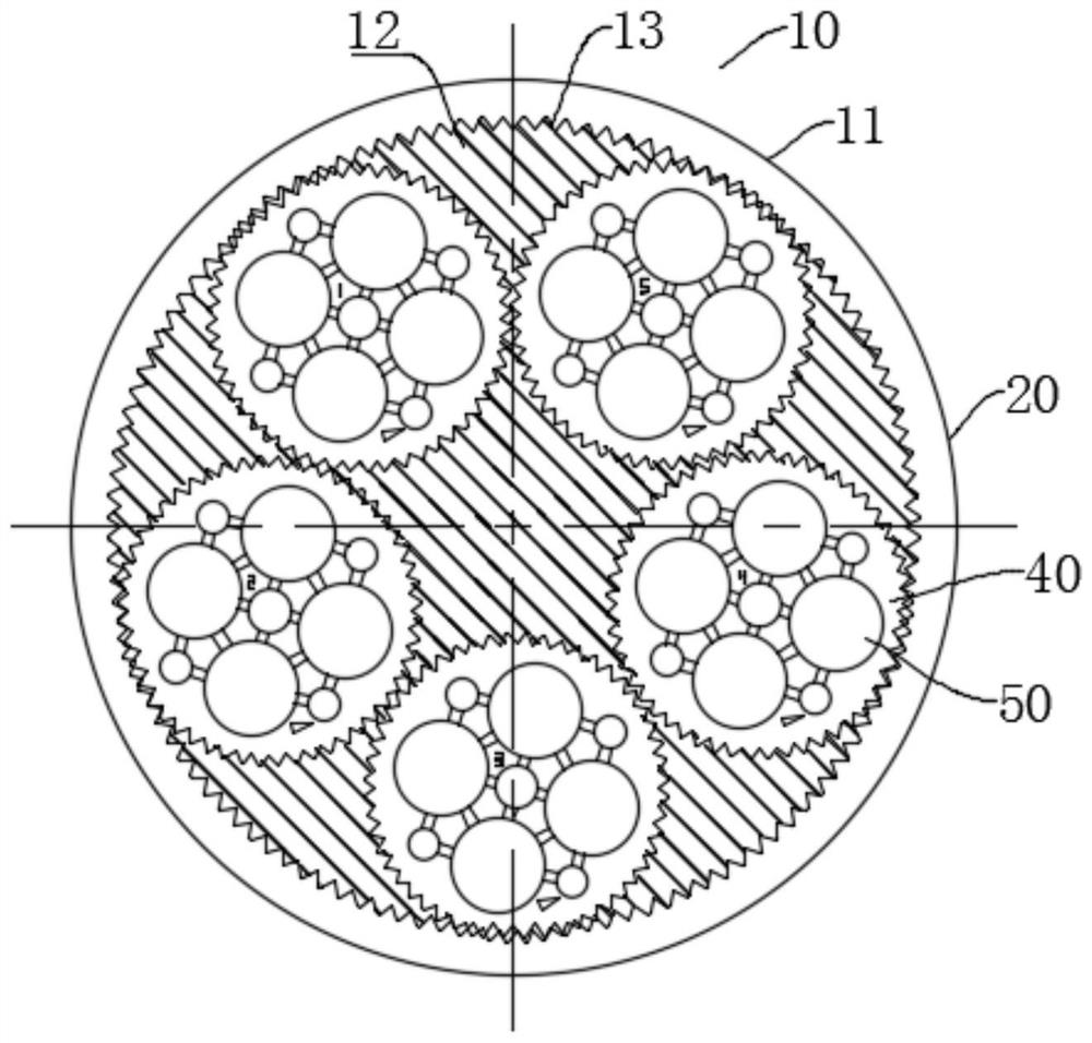
[0037] This embodiment proposes a double-sided polishing device for large-size silicon wafers, such as figure 1 As shown, it includes a carrier assembly 10 for placing a silicon wafer 50, a pressure plate 20 adapted to the carrier assembly 10 and in contact with the upper end surface of the silicon wafer 50, and a liquid casting assembly 30 that can provide rough or fine liquid. Single or several silicon wafers 50 are placed in the carrier assembly 10; the liquid throwing assembly 30 provides rough or fine throwing liquid to both sides of the silicon wafer 50 through the pressure plate 20, and the rough or fine throwing liquid is carried by the carrying assembly 10 and The counter-rotating force of the pressure plate 20 drives and rotates with the rotation of the silicon wafer 50 to polish both sides of the silicon wafer 50 .

[0038] Such a...


PUM

PropertyMeasurementUnit
particle diameteraaaaaaaaaa
sizeaaaaaaaaaa
surface smoothnessaaaaaaaaaa

Abstract

The invention provides a large-size silicon wafer double-sided polishing method. The method comprises the following steps of: controlling the pressure of a pressure plate arranged above a silicon wafer, and selecting a rough polishing solution with a corresponding particle size to roughly polish the double sides of the silicon wafer; and adjusting the pressure of the pressure plate, and selecting a fine polishing solution with a corresponding particle size to carry out fine polishing on the double sides of the silicon wafer, wherein the rough polishing solution or the fine polishing solution flows to an upper polishing pad and a lower polishing pad which are arranged on the two sides of the silicon wafer through the same main pipeline and the pressure plate; the fine polishing solution at least comprises a polyhydric alcohol compound; and the rough polishing solution and the fine polishing solution both comprise a mixed solution of SiO2 and NH4OH. After rough polishing and fine polishing are sequentially conducted on the silicon wafer, water film treatment is conducted on the double sides of the silicon wafer, an adhesive on the surface of the silicon wafer can be completely removed, and the cleaning effect is good; and the flatness within 0.5 [mu]m can also be obtained.

Description

technical field [0001] The invention belongs to the technical field of semiconductor silicon wafer polishing, and in particular relates to a large-size silicon wafer double-sided polishing method. Background technique [0002] Existing semiconductor polishing methods are mainly single-side polishing, which is only suitable for small-sized silicon wafers with a size of 4-8 inches. With the development of large-scale solar silicon wafers, for 12-inch and more than 12-inch silicon wafers, the larger the single-sided size of the silicon wafer, the more difficult it is to control the geometric parameters of its polishing; at the same time, if single-sided polishing is used In this way, not only the polishing efficiency is low, but also the polishing quality is difficult to guarantee. The flatness of the geometric parameters after polishing has a large variation range and poor consistency, which does not meet the standard requirements and seriously affects the processing of semico...

Claims


Application Information

Patent Timeline
Patent Type & Authority Applications(China)
IPC IPC(8): B24B29/02B24B27/00B24B41/00B24B41/06B24B47/12B24B57/02
CPCB24B29/02B24B27/0076B24B27/0023B24B47/12B24B57/02B24B41/007B24B41/06
Inventor 祝斌武卫刘建伟刘园刘姣龙裴坤羽杨春雪由佰玲孙晨光王彦君常雪岩谢艳袁祥龙张宏杰刘秒吕莹徐荣清
Owner TIANJIN ZHONGHUAN ADVANCED MATERIAL TECH
Why Eureka
Try Eureka