Production method of AlSb-GeSn-AlSb heterostructure solid-state plasma PiN diode and device thereof
A plasma and heterostructure technology, applied in semiconductor/solid-state device manufacturing, semiconductor devices, electrical components, etc., can solve the problem of low gain of silicon-based reconfigurable antennas, low diode carrier concentration, and poor distribution uniformity, etc. problems, to achieve the effect of improving system integration and stealth performance, improving concentration and distribution uniformity, and increasing junction depth
- Summary
- Abstract
- Description
- Claims
- Application Information
AI Technical Summary
Problems solved by technology
Method used
Image


Examples
Embodiment 1
[0067] See figure 1 , figure 1 It is a flowchart of a method for manufacturing a solid-state plasma PiN diode with an AlSb-GeSn-AlSb heterostructure according to an embodiment of the present invention. The method is suitable for preparing a lateral solid-state plasma PiN diode based on GeOI, and the AlSb-GeSn-AlSb heterostructure Solid-state plasmonic PiN diodes with solid structures are mainly used to make silicon-based highly integrated reconfigurable antennas. The method comprises the steps of:
[0068] (a) Selecting a GeOI substrate with a certain crystal orientation, and doping in the GeOI substrate to form a top-layer GeSn region;
[0069] (b) setting a deep trench isolation region in the GeSn region on the top layer of the substrate;
[0070] (c) etching the GeSn region to form a P-type trench and an N-type trench, and the depth of the P-type trench and the N-type trench is less than the thickness of the top-layer GeSn region;
[0071] (d) forming a P-type active re...
Embodiment 2
[0111] See Figure 2a-Figure 2t , Figure 2a-Figure 2t It is a schematic diagram of a method for preparing a solid-state plasma PiN diode with an AlSb-GeSn-AlSb heterostructure according to an embodiment of the present invention. A solid-state plasma PiN diode with an AlSb-GeSn-AlSb heterostructure between 50 microns and 150 microns) can be used as an example to describe in detail, and the specific steps are as follows:
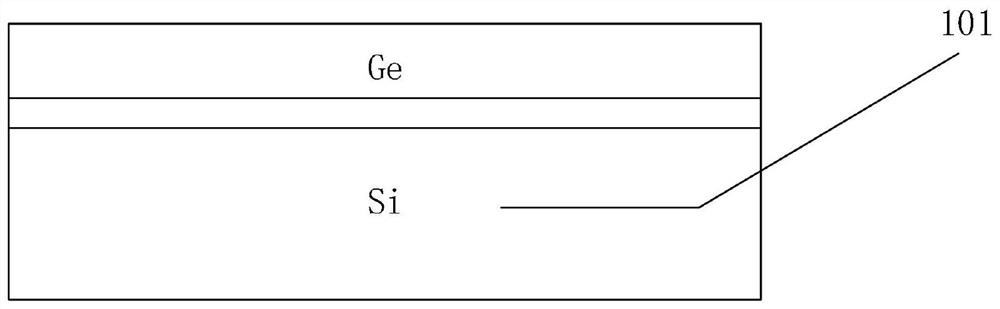
[0112] S10, selecting a GeOI substrate.
[0113] See Figure 2a , the crystal orientation of the GeOI substrate 101 may be (100) or (110) or (111), without any limitation here. In addition, the doping type of the GeOI substrate 101 can be n-type or p-type, and the doping concentration is, for example, 0.5×10 14 ~0.5×10 15 cm -3 , the thickness of the top layer Ge is, for example, 30-120 μm.
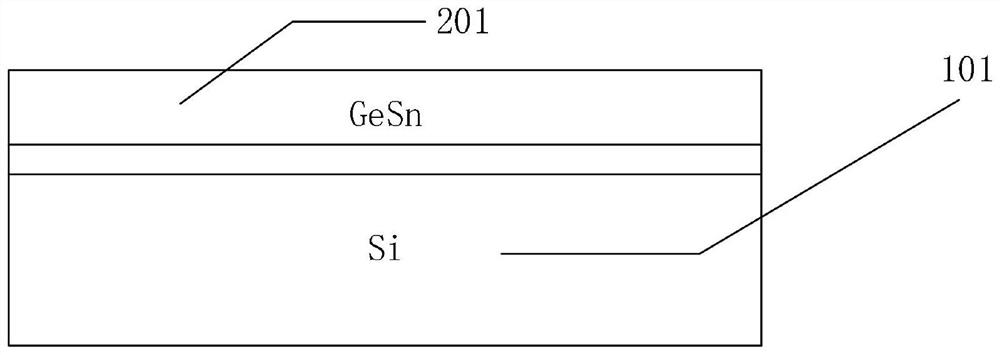
[0114] S20, doping in the GeOI substrate to form a top-layer GeSn region.
[0115] See Figure 2b The specific method may be: photoetching the GeOI substrate, d...
Embodiment 3
[0155] Please refer to image 3 , image 3 It is a schematic diagram of the device structure of the AlSb-GeSn-AlSb heterostructure solid-state plasmonic PiN diode according to the embodiment of the present invention. The AlSb-GeSn-AlSb heterostructure PiN diode adopts the above-mentioned figure 1 The preparation method shown is made, specifically, the solid-state plasma PiN diode of the AlSb-GeSn-AlSb heterostructure is prepared and formed on the GeOI substrate 301, and the P region 303, the N region 304 of the diode and the lateral direction are located on the P The intrinsic region between region 303 and the N region 304 is located in the top GeSn layer 302 of the substrate. Wherein, the PiN diode adopts deep trench isolation technology, that is, a deep trench isolation region 307 is provided outside the P region 303 and the N region 304, and the depth of the isolation trench 307 is greater than or equal to the thickness of the top GeSn layer 302. In addition, the P regio...
PUM
| Property | Measurement | Unit |
|---|---|---|
| thickness | aaaaa | aaaaa |
| thickness | aaaaa | aaaaa |
Abstract
Description
Claims
Application Information
 - Generate Ideas
- Intellectual Property
- Life Sciences
- Materials
- Tech Scout
- Unparalleled Data Quality
- Higher Quality Content
- 60% Fewer Hallucinations
Browse by: Latest US Patents, China's latest patents, Technical Efficacy Thesaurus, Application Domain, Technology Topic, Popular Technical Reports.
© 2025 PatSnap. All rights reserved.Legal|Privacy policy|Modern Slavery Act Transparency Statement|Sitemap|About US| Contact US: help@patsnap.com