High-voltage low-resistance power LDMOS

A power-resistance and high-voltage technology, applied in the field of power semiconductors, to achieve the effect of large breakdown voltage and small specific on-resistance

Active Publication Date: 2021-06-04
UNIV OF ELECTRONICS SCI & TECH OF CHINA
View PDF5 Cites 1 Cited by
  • Summary
  • Abstract
  • Description
  • Claims
  • Application Information

AI Technical Summary

Problems solved by technology

However, whether it is slot technology, super junction technology or RESURF technology, the current in forward conduction is the drift transport mode of carriers passing through the neutral drift region, so R on,sp will still be constrained by the doping concentration in the drift region

Method used


Image

  • High-voltage low-resistance power LDMOS
  • High-voltage low-resistance power LDMOS
  • High-voltage low-resistance power LDMOS

Examples


Embodiment 1

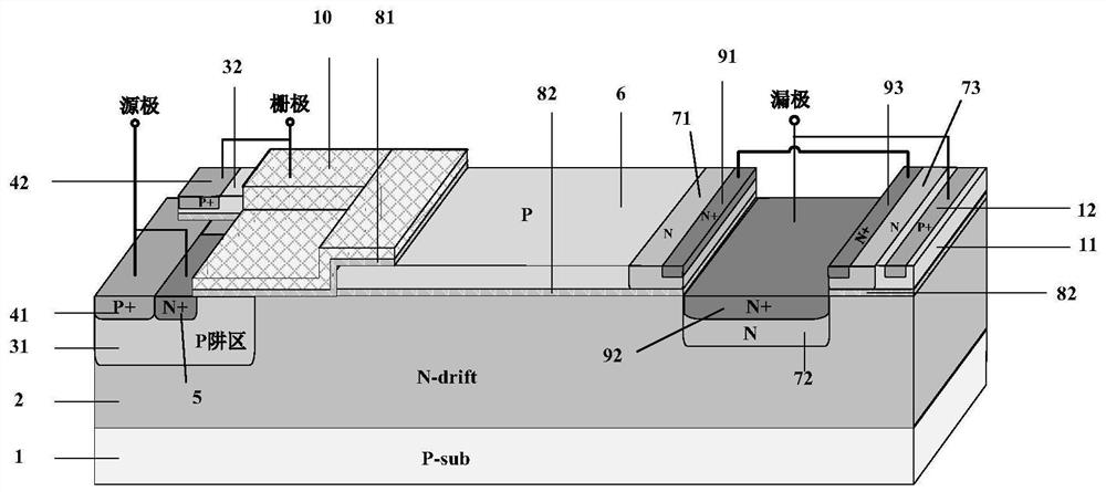
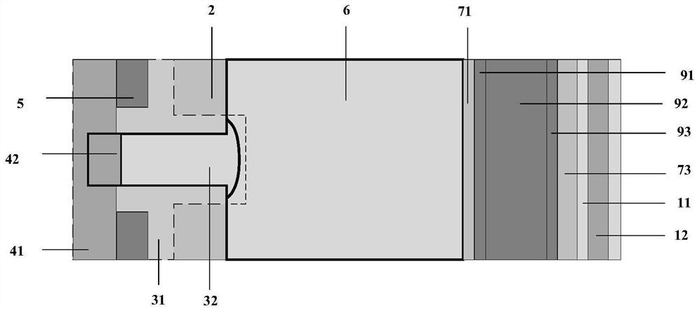
[0020] like figure 1 , 2 As shown, it is a high-voltage low-resistance power LDMOS in this example, which includes a P substrate 1, an N drift region 2, and a top-layer structure that are sequentially stacked from bottom to top along the vertical direction of the device. The top-layer structure includes a field plate structure and an integrated Diode structure;

[0021] Along the lateral direction of the device, the surface of the N drift region 2 includes a source structure, a gate structure, and a drain structure from one side to the other; the field plate structure and the integrated diode are respectively located on both sides of the drain structure, and the The field plate structure is located between the source structure and the drain structure;

[0022] The source structure includes a P well region 31, a P+ body contact region 41, and a first N+ heavily doped region 5; the P+ body contact region 41 and the first N+ heavily doped region 5 are in contact with each other...

Embodiment 2

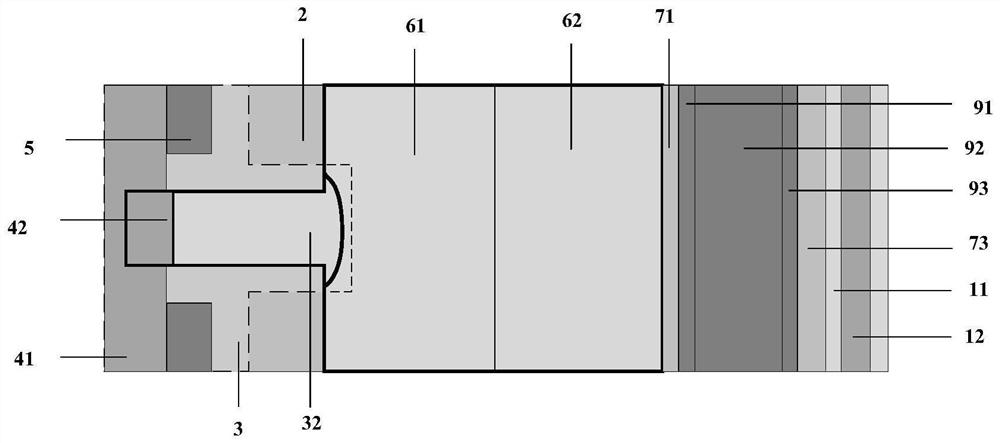
[0029] like image 3 As shown, the difference between this example and Example 1 is that in the field plate structure described in this example, the P-type region 6 includes a first P+ heavily doped region 42 from the source terminal to the drain terminal along the lateral direction of the device, a P well doped impurity region 32, P-type first-order doped region 61, P-type second-order doped region 62, N-doped region 71 and third N+ heavily doped region 91; wherein P-type first-order doped region 61 and P-type second-order doped region The doping concentration of the step-doped region 62 is from high to low in the direction from the source structure to the drain structure.

[0030] Compared with Embodiment 1, the field plate structure has a better effect on modulating the lateral electric field distribution of the device, and this embodiment can obtain a higher withstand voltage under the same device size.


PUM


Abstract

The invention belongs to the technical field of power semiconductors, and particularly relates to a high-voltage low-resistance power LDMOS. The LDMOS is mainly characterized by being provided with a field plate structure with a protruding source end and an integrated diode on the inner side of a drain electrode, the length of a drift region is shortened, and the device area is not additionally increased. During forward conduction, an integrated diode is reversely biased, a field plate structure and an N-type drift region form an equivalent MIS capacitor, a continuous electron accumulation layer is generated on the surface of the drift region below a gate structure and the field plate structure, an accumulation type transport mode is formed, and the specific on-resistance of the device is greatly reduced; during reverse blocking, the integrated diode is positively biased, the field plate structure bears surface withstand voltage, the drift region is assisted to be depleted so as to improve the doping concentration of the drift region and reduce the specific on-resistance, and transverse electric field distribution is modulated so as to improve the withstand voltage of the device. Compared with a traditional LDMOS, the LDMOS provided by the invention has lower specific on-resistance while realizing high withstand voltage.

Description

technical field [0001] The invention belongs to the technical field of power semiconductors, and relates to a high-voltage low-resistance power LDMOS (Lateral DoubleDiffusion MOS, lateral double-diffusion metal oxide semiconductor field effect transistor). Background technique [0002] Compared with VDMOS (Vertical Double Diffusion MOS, vertical double diffused metal oxide semiconductor field effect transistor), LDMOS has the characteristics of fast switching speed and easy integration, and is widely used in power integrated circuits. [0003] In conventional LDMOS, there is a specific on-resistance (Special On-resistance, R on,sp ) and the contradictory relationship between the breakdown voltage (Breakdown Voltage, BV): R on,sp ∝BV 2.5 , which is called the "silicon limit". By reducing the doping concentration of the drift region and increasing the drift region, the withstand voltage of the device can be improved, but at the same time, the specific on-resistance of the d...

Claims


Application Information

Patent Timeline
IPC IPC(8): H01L29/40H01L29/423H01L29/78
CPCH01L29/402H01L29/42356H01L29/7818
Inventor 魏杰戴恺纬李杰马臻李聪聪罗小蓉
Owner UNIV OF ELECTRONICS SCI & TECH OF CHINA
Why Eureka
Try Eureka