
Semiconductor laser with stepped waveguide thickness

A step wave and laser technology, which is applied in the direction of semiconductor lasers, optical waveguide semiconductor structures, lasers, etc., can solve the problem of increased threshold current density in the MO region, reduced difference between fast-axis fundamental mode and higher-order mode threshold, and increased difficulty in preparing on-chip gratings. question

Inactive Publication Date: 2021-05-18
INST OF APPLIED ELECTRONICS CHINA ACAD OF ENG PHYSICS
View PDF5 Cites 0 Cited by
  • Summary
  • Abstract
  • Description
  • Claims
  • Application Information

AI Technical Summary

Problems solved by technology

[0004] However, for on-chip MOPA integration, the main disadvantages of the EDAS structure are as follows: 1. The MO region needs to prepare a single-mode narrow ridge structure. The threshold difference is reduced, and high-order mode lasing is easy to occur; 2. The low mode confinement factor increases the threshold current density of the MO region; 3. The MO region needs to prepare an on-chip grating to generate resonance, and the EDAS structure makes the optical field biased towards the N measurement distribution, reducing The coupling between the on-chip grating and the light field increases the difficulty of preparing the on-chip grating
[0005] In summary, for the on-chip integrated MOPA structure, the MO region and the PA region have different requirements for the thickness of the epitaxial waveguide. It is difficult to use a unified epitaxial structure to play a good role in the two regions at the same time, which is very unfavorable for the preparation of high-performance semiconductor MOPA devices.

Method used


Image

  • Semiconductor laser with stepped waveguide thickness

Examples


Embodiment 1

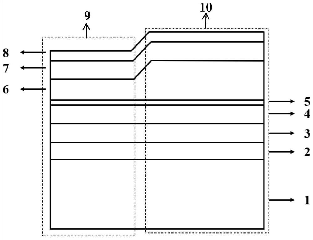
[0032]In this embodiment, a semiconductor laser with stepped waveguide thickness is specifically disclosed, aiming to solve the problem that the existing unified waveguide structure is difficult to simultaneously meet the requirements of the on-chip structure for fast-axis mode control and power amplification. Such as figure 1 As shown, the semiconductor laser should include a substrate layer, with the substrate layer as the base layer, the semiconductor laser also includes:

[0033] The buffer layer, lower confinement layer, lower waveguide layer, quantum well active layer, upper waveguide layer, upper confinement layer and ohmic contact layer are arranged sequentially from bottom to top on the surface of the substrate layer, and the upper waveguide layer, upper confinement layer layer and the ohmic contact layer together form an epitaxial structure with a step thickness. The advantage of this design method is that when the MOPA is integrated on-chip, a waveguide structure w...


PUM

PropertyMeasurementUnit
Thicknessaaaaaaaaaa
Thicknessaaaaaaaaaa
Thicknessaaaaaaaaaa

Abstract

The invention discloses a semiconductor laser with stepped waveguide thickness, and belongs to the technical field of semiconductor photoelectrons. The laser comprises a substrate layer, a buffer layer, a lower limiting layer, a lower waveguide layer, a quantum well active layer, an upper waveguide layer, an upper limiting layer and an ohmic contact layer from bottom to top. Different upper waveguide thicknesses on two sides of a corrosion interface are formed on an upper waveguide layer by adopting a selective region corrosion and secondary epitaxial process, and a secondary epitaxial waveguide thickness is adopted, so that an integrated laser on a preparation chip is facilitated, a corrosion region is of a small optical cavity epitaxial structure, a non-corrosion region is of a large optical cavity epitaxial structure, a small optical cavity epitaxial structure can accommodate a small number of modes, and high-order mode lasing is effectively inhibited; the fundamental mode limiting factor of the small optical cavity is high, so that the threshold current density of the area is effectively reduced; and the large optical cavity is a laser emitting cavity surface, which is beneficial to reducing the laser power density of the cavity surface and improving the saturation output power.

Description

technical field [0001] The invention belongs to the technical field of semiconductor optoelectronics, and in particular relates to a semiconductor laser with stepped waveguide thickness. Background technique [0002] High-power semiconductor lasers have the advantages of small size, high electro-optic conversion efficiency, and easy integration. They are widely used in civil and military fields such as medical treatment, machining, communication, guidance, solid-state lasers, and fiber laser pumps. However, the beam quality control of semiconductor lasers is always a technical difficulty in its direct application. In recent years, thanks to the research on the structure of the main oscillator power amplifier (MOPA), the high power output of semiconductor lasers near the diffraction limit has been effectively realized. Among them, on-chip integrated MOPA can give full play to the advantages of light weight of semiconductor lasers and reduce the system complexity brought by t...

Claims


Application Information

Patent Timeline
IPC IPC(8): H01S5/20H01S5/343
CPCH01S5/2004H01S5/343
Inventor 何林安周坤杜维川李弋高松信唐淳
Owner INST OF APPLIED ELECTRONICS CHINA ACAD OF ENG PHYSICS
Learn More