LNOI spot size converter based on sub-wavelength grating, and preparation method
A technology of sub-wavelength grating and mode-spot converter, which is applied in the direction of optical waveguide light guide, optical waveguide coupling, instrument, etc., can solve problems such as difficult LNOI optical chip production, limited optical mode field amplification ability, and weakened limitation ability, etc., to achieve Promote practical application, reduce effective refractive index, and reduce the effect of refractive index difference
- Summary
- Abstract
- Description
- Claims
- Application Information
AI Technical Summary
Problems solved by technology
Method used
Image

Examples
preparation example Construction
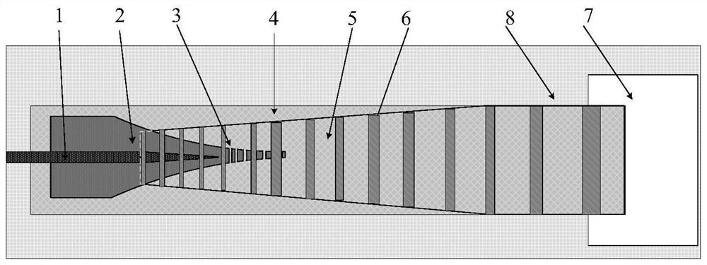
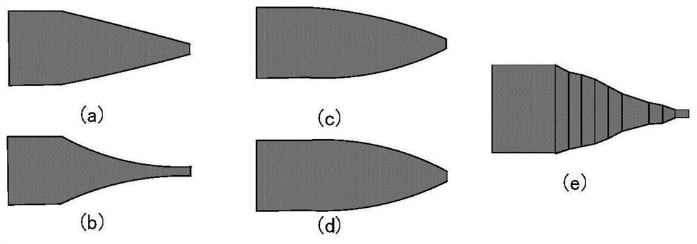
[0054]Such asFigure 6The process steps of the preparation method of the LnOI mold converter of the present invention include the following steps:
[0055]Step S1, the top tapered waveguide 1 etching mask was prepared. Waveguide etch masks include photoresist and metal masks, photoresist including HSQ negative glue, ZEP 520a positive colloid and 7908 positive glue, metal mask material is Ni or Ti / Ni, or Cr / Ni.
[0056]Step S2, the top tapered waveguide 1 etch. Waveguide etching uses dry etching processes, using reaction ion etching or inductively coupled plasma etching, etching gas is Ar, or sf6 / Ar mixed gas.
[0057]Step S3, the underlying cone waveguide 2 and the tapered sub-wavelength grating 3 etching mask was prepared.
[0058]Step S4, the underlying cone waveguide 2 and the conical sub-wavelength grating 3 etch.
[0059]Step S5, SIO2Medium growth: Growing SIO with PECVD2SiO2The thickness is 1 μm to 2 μm.
[0060]Step S6, SiN media growth: The SiN is grown by PECVD, and the thickness of SiN ...
Embodiment 1
[0067]The 3-inch x-cut lnoi wafer is selected, the lithium niobate film has a thickness of 600 nm, SiO2The insulating layer has a thickness of 2 μm, the substrate is Si material, and the preparation process step is:
[0068]A1) Top-tapered waveguide 1 etch mask preparation: spin coating negative HSQ, the rotational speed is 2000 rpm / min, baked for 120 seconds at 150 ° C hot plate.
[0069]A2) Top-tapered waveguide 1 etch: Ar plasma ICP etching, waveguide etching depth is 300 nm.
[0070]A3) The underlying cone waveguide 2 and the conical sub-wavelength grating 3 etch mask was prepared: spin coating negative HSQ, the rotational speed was 2000 rpm / min, baked on the heat plate of 150 ° C for 120 seconds.
[0071]A4) The underlying cone waveguide 2 and the conical sub-wavelength grating 3 etch: AR plasma ICP dry etching, the waveguide etching depth is 300 nm.
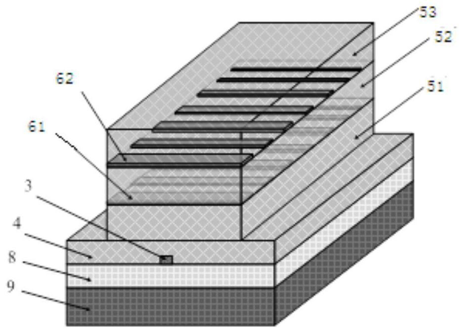
[0072]A5) First SIO2Package 51 Media Growth: PECVD Growth SiO2The cladding medium with a thickness of 1 μm.
[0073]A6) The first layer SiN s...
Embodiment 2
[0080]The 3-inch x-cut lnoi wafer is selected, the lithium niobate film has a thickness of 600 nm, SiO2The insulating layer has a thickness of 2 μm, the substrate is Si material, and the main preparation process step is:
[0081]B1) Top-tapered waveguide 1 etch mask preparation: spin coating photoresist 7908, exposure development After evaporation of metal Ti / Ni20 / 150 nm, soaked in acetone, ultrasonic removal of photoresist, then in ethanol for 5 minutes, then Rinse it with deionized water, and finally put it in the dryer.
[0082]B2) Top-tapered waveguide 1 etch: AR plasma ICP etching, waveguide etching depth is 300 nm.
[0083]B3) Bottomatal cone waveguide 2 and sub-wavegoon 3 etch mask Preparation: Cerectant photoresist 7908, exposure development After evaporation of metal Ti / Ni 20 / 150 nm, and soak it with acetone, ultrasonic removal photoresist, then in ethanol The ultrasound is less than 5 minutes, then rinsed with deionized water, and finally put it in the dryer.
[0084]B4) The und...
PUM
| Property | Measurement | Unit |
|---|---|---|
| Waveguide width | aaaaa | aaaaa |
| Length | aaaaa | aaaaa |
| Width | aaaaa | aaaaa |
Abstract
Description
Claims
Application Information
 - R&D
- Intellectual Property
- Life Sciences
- Materials
- Tech Scout
- Unparalleled Data Quality
- Higher Quality Content
- 60% Fewer Hallucinations
Browse by: Latest US Patents, China's latest patents, Technical Efficacy Thesaurus, Application Domain, Technology Topic, Popular Technical Reports.
© 2025 PatSnap. All rights reserved.Legal|Privacy policy|Modern Slavery Act Transparency Statement|Sitemap|About US| Contact US: help@patsnap.com