
Slide glass structure with side wall bonding pad, and manufacturing method thereof

A manufacturing method and pad technology, applied in the use/removal method of circuit masks, printed circuit manufacturing, coupling of optical waveguides, etc., can solve the problems of large difficulty, large coupling space between optical fiber and circuit board, and unfavorable module miniaturization And other issues

Active Publication Date: 2021-04-23
NAT CENT FOR ADVANCED PACKAGING
View PDF7 Cites 1 Cited by
  • Summary
  • Abstract
  • Description
  • Claims
  • Application Information

AI Technical Summary

Problems solved by technology

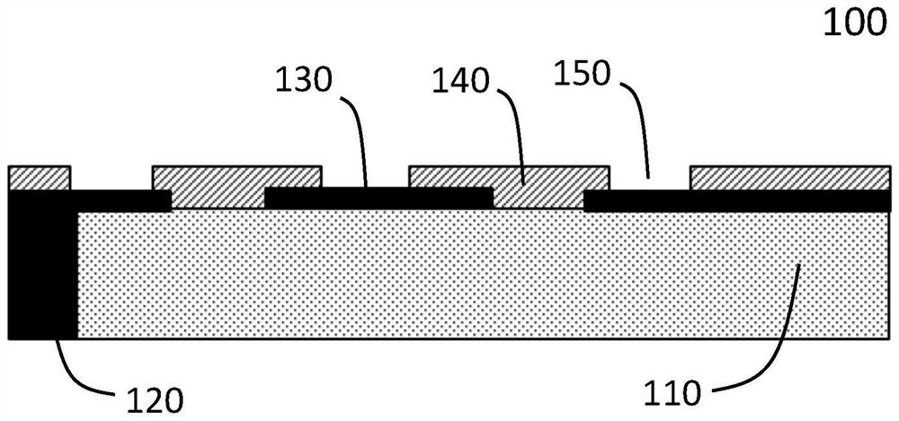
[0005] Aiming at the problems of large coupling space between the existing optical fiber and the circuit board, which is not conducive to the miniaturization of modules, and the problems of difficulty, high cost and poor reliability in the prior art, according to an embodiment of the present invention, a belt-side Carrier structure for wall pads, including:

Method used


Image

  • Slide glass structure with side wall bonding pad, and manufacturing method thereof
  • Slide glass structure with side wall bonding pad, and manufacturing method thereof
  • Slide glass structure with side wall bonding pad, and manufacturing method thereof

Examples


Embodiment Construction

[0033] In the following description, the present invention is described with reference to various examples. One skilled in the art will recognize, however, that the various embodiments may be practiced without one or more of the specific details, or with other alternative and / or additional methods, materials, or components. In other instances, well-known structures, materials, or operations are not shown or described in detail so as not to obscure aspects of the various embodiments of the invention. Similarly, for purposes of explanation, specific quantities, materials and configurations are set forth in order to provide a thorough understanding of embodiments of the invention. However, the invention may be practiced without these specific details. Furthermore, it should be understood that the various embodiments shown in the drawings are illustrative representations and are not necessarily drawn to scale.

[0034] In this specification, reference to "one embodiment" or "the...


PUM


Abstract

The invention discloses a slide glass structure with a side wall bonding pad. The structure comprises: a dielectric substrate which is a substrate of the slide glass structure of the side wall bonding pad; a sidewall pad, wherein the side wall bonding pad is arranged on the side wall of the dielectric substrate and extends from the bottom surface to the top surface along the side wall of the dielectric substrate; a surface metal wiring layer, arranged on the top surface of the dielectric substrate and electrically connected to the side wall bonding pad; a surface dielectric layer arranged on the top surface of the dielectric substrate and above part of the surface metal wiring layer; and a surface dielectric layer window, wherein a part of the surface metal wiring layer is exposed from the surface dielectric layer window.

Description

technical field [0001] The invention relates to the technical field of semiconductor packaging, in particular to a chip carrier structure with sidewall pads and a manufacturing method thereof in the technical field of photoelectric packaging. Background technique [0002] In the photoelectric coupling system, the vertical cavity surface emitting laser (VCSEL) and the surface photodetector are generally directly aligned and coupled with the optical fiber. Although this coupling method has high efficiency, the direction of the optical fiber and the surface of the circuit board are perpendicular to each other. The bending half of the ribbon is relatively large, so the application scenario of this coupling method usually needs to reserve a large space in the vertical direction of the circuit board plane. The space requirements for the size are obviously not conducive to the development of module miniaturization. [0003] In order to achieve direct vertical alignment coupling bet...

Claims


Application Information

Patent Timeline
Patent Type & Authority Applications(China)
IPC IPC(8): H05K1/02H05K1/11H05K3/00G02B6/42
CPCH05K1/02H05K1/0296H05K1/117H05K3/00H05K3/0079G02B6/428
Inventor 张凯曹立强
Owner NAT CENT FOR ADVANCED PACKAGING
Learn More