Antimony telluride photoelectric detector and production method thereof
A photodetector and photodetection technology, which is applied in the fields of electrical solid-state devices, semiconductor/solid-state device manufacturing, photovoltaic power generation, etc., can solve the problems of insufficient response rate and insufficient response band, and achieve high electron mobility and preparation cycle short effect
- Summary
- Abstract
- Description
- Claims
- Application Information
AI Technical Summary
Problems solved by technology
Method used
Image

Examples
Embodiment 1
[0032] In this embodiment, PbPc / Sb 2 Te 3 / n-Si heterojunction linear array thin film photodetector preparation method is described, in which Sb 2 Te 3 As a light absorbing material, n-Si is used as the substrate and Sb 2 Te 3 A heterojunction in the vertical direction is formed, and PbPc acts as a light-enhanced absorbing material.
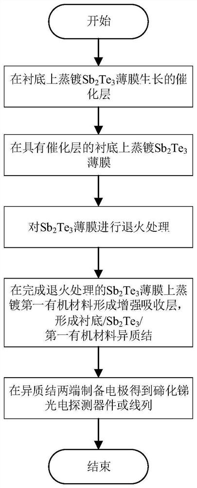
[0033] Such as figure 1 Shown, in embodiment 1, a kind of preparation method of antimony telluride photodetection device specifically comprises the following steps:
[0034] S01: Evaporate Sb on the substrate 2 Te 3 The catalytic layer of film growth; wherein, the substrate is any one of silicon oxide wafer, silicon wafer, fluorine phlogopite, and quartz, and the present embodiment adopts n-Si of 1.5cm×1.5cm as the substrate, and the substrate Put in acetone, alcohol, and deionized water for 30 minutes to ultrasonically remove organic and inorganic impurities on the surface of the substrate, and then put it in a UV cleaning machine for 30...
Embodiment 2
[0049] In this example, Sb 2 Te 3 / C 60 / CuPc heterojunction thin film photodetectors were prepared, in which Sb 2 Te 3 As a light absorbing material, C 60 with Sb 2 Te 3 Forming a heterojunction in the vertical direction, CuPc acts as a light-enhanced absorbing material, such as figure 1 Shown, in embodiment 2, a kind of preparation method of antimony telluride photodetection device specifically comprises the following steps:
[0050] S11: Evaporate Sb on the substrate 2 Te 3 The catalytic layer of film growth; wherein, the substrate is any one of silicon oxide wafer, silicon wafer, fluorine phlogopite, and quartz, and the present embodiment adopts an oxygen silicon wafer of 1.5cm×1.5cm as the substrate, and Put in acetone, alcohol, and deionized water for 30 minutes to ultrasonically remove organic and inorganic impurities on the surface of the substrate, and then put it in a UV cleaning machine for 30 minutes to make the surface of the substrate hydrophilic.
[00...
Embodiment 3
[0064] This embodiment has the same inventive concept as Embodiment 1. On the basis of Embodiment 1, a kind of antimony telluride photodetection device is provided, such as Figure 5 As shown, the device includes from bottom to top: substrate, Sb 2 Te 3 A thin film layer, a first organic material layer and an electrode. The substrate is n-Si, the first organic material is PbPc, Sb 2 Te 3 thin film with the first organic material to form Sb 2 Te 3 / PbPc heterojunction, and vapor-deposit multiple Au electrodes on both ends of the heterojunction (n-Si substrate, PbPc film) to obtain patterned PbPc / Sb 2 Te 3 / n-Si heterojunction photodetection unit device.
[0065] It should be noted, Figure 5 Among them, 1 is n-Si substrate, 2 is Sb 2 Te 3 / PbPc heterojunction, 3 is Au electrode.
PUM
| Property | Measurement | Unit |
|---|---|---|
| Thickness | aaaaa | aaaaa |
Abstract
Description
Claims
Application Information
 - Generate Ideas
- Intellectual Property
- Life Sciences
- Materials
- Tech Scout
- Unparalleled Data Quality
- Higher Quality Content
- 60% Fewer Hallucinations
Browse by: Latest US Patents, China's latest patents, Technical Efficacy Thesaurus, Application Domain, Technology Topic, Popular Technical Reports.
© 2025 PatSnap. All rights reserved.Legal|Privacy policy|Modern Slavery Act Transparency Statement|Sitemap|About US| Contact US: help@patsnap.com