Micro-nano composite structure photon integrated chip and preparation method thereof

A technology of micro-nano composite structure and photonic integration, applied in final product manufacturing, sustainable manufacturing/processing, electrical components, etc. Improve the communication rate, increase the degree of overlap of the response spectrum, and reduce the effect of the Stokes effect

Active Publication Date: 2021-03-26
NANJING UNIV OF POSTS & TELECOMM
View PDF4 Cites 3 Cited by
  • Summary
  • Abstract
  • Description
  • Claims
  • Application Information

AI Technical Summary

Problems solved by technology

[0005] Although some progress has been made in photonic integrated chips, there are still some challenging problems in order to achieve large-scale commercialization. The overlapping degree of the emission spectrum and the response spectrum of the detector is small, which leads to problems such as low communication rate

Method used


Image

  • Micro-nano composite structure photon integrated chip and preparation method thereof
  • Micro-nano composite structure photon integrated chip and preparation method thereof
  • Micro-nano composite structure photon integrated chip and preparation method thereof

Examples


Embodiment 1

[0059] A method for preparing a photonic integrated chip with a micro-nano composite structure, the steps comprising:

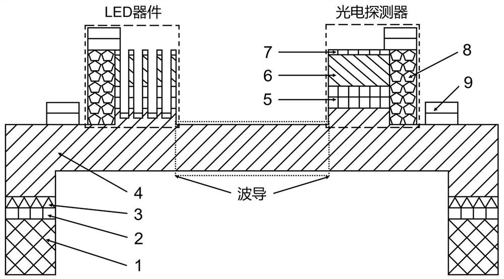
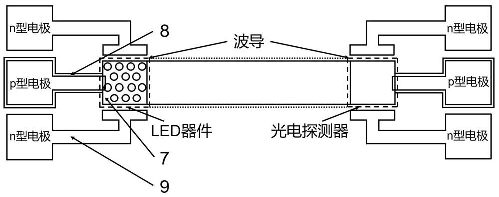
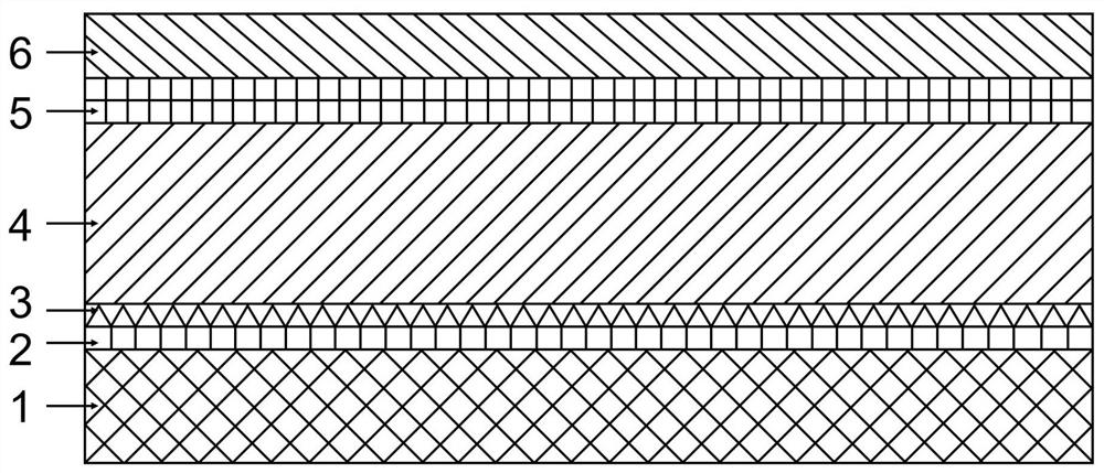
[0060] (1) On the silicon substrate layer 1, a buffer layer 2, an undoped GaN layer 3, an n-type GaN layer 4, an InGaN / GaN multi-quantum well layer 5, and a p-type GaN layer 6 are sequentially grown to prepare an InGaN / GaN multi-quantum well LED epitaxial wafer; InGaN / GaN multi-quantum well LED epitaxial wafer, the In composition is 0.2, the light emission wavelength is 450nm, the period number of InGaN / GaN multi-quantum well layer 5 is 5, the thickness of the InGaN well layer is 3 nm, and the GaN barrier The thickness of the layer is 10 nm; the thickness of the p-type GaN layer 6 is 200 nm;

[0061] (2) Thinning and polishing the back of the silicon substrate layer 1 on the InGaN / GaN multi-quantum well LED epitaxial wafer, and using plasma enhanced chemical vapor deposition (PECVD) to grow a layer 2 on the surface of the InGaN / GaN multi-quantum well LED epit...


PUM

PropertyMeasurementUnit
wavelengthaaaaaaaaaa
thicknessaaaaaaaaaa
emission peakaaaaaaaaaa

Abstract

The invention discloses a micro-nano composite structure photon integrated chip and a preparation method thereof, and belongs to the technical field of semiconductor photoelectronic devices and integration, a chip uses a nano preparation technology to obtain a nano LED structure, then uses a photoetching technology to obtain an LED device, a waveguide and a photoelectric detector, and uses a deepsilicon etching technology and a nitride back etching technology to obtain the ultrathin silicon substrate suspended micro-nano composite structure photon integrated chip. According to the chip, the nanostructure LED device, the waveguide and the photoelectric detector are integrated on the same chip, light emitted by the nanostructure LED device is laterally coupled into the waveguide, transmitted through the waveguide and detected by the photoelectric detector at the other end of the waveguide, the nanostructure can enhance the modulation bandwidth of an LED and increase the overlapping degree of a light-emitting spectrum of the LED and a response spectrum of the detector, and the high-speed photonic integrated chip is applied to the fields of optical communication and optical sensing.

Description

technical field [0001] The invention belongs to the technical field of semiconductor optoelectronic devices and integration, and in particular relates to a photon integrated chip with a micro-nano composite structure and a preparation method thereof. Background technique [0002] Visible light communication is an optical communication technology developed based on the high switching response of light-emitting diodes (LEDs). Using its high-speed response characteristics of output optical power and driving current, visible light is used as an information carrier to directly transmit optical signals in transmission media such as air. Compared with traditional wireless communication, a communication method has attracted much attention due to its advantages such as wide spectrum, high transmission power, harmless to human body, no electromagnetic interference, and good confidentiality. [0003] With the continuous development of visible light communication technology and the cont...

Claims


Application Information

Patent Timeline
Patent Type & Authority Applications(China)
IPC IPC(8): H01L27/15H01L31/0232H01L31/18H01L33/00H01L33/06H01L33/32
CPCH01L27/15H01L31/02327H01L31/1848H01L33/007H01L33/06H01L33/325Y02P70/50
Inventor 张国刚金志远陈宇飞葛海涛王永进
Owner NANJING UNIV OF POSTS & TELECOMM
Why Eureka
Try Eureka