


Quick Research
Generate reliable direction feasibility study reports for your R&D in just a few steps.

Technical Q&A
Discover and master advanced knowledge NOW. Basics, ideas, possibilities, all at once.

Find Solutions
As an expert in R&D theories, this can generate solutions to your technical problems instantly.

Evaluate Feasibility
Analyze your overall solution with one click, know your potential R&D risks in advance.

Monitor Landscape
Get weekly tech updates, stay abreast of the latest tech innovations and key insights.
Bidirectional voltage-stabilizing electrostatic surge full-chip protection integrated circuit
A bidirectional voltage regulation, integrated circuit technology, applied in circuits, electrical components, electrical solid devices, etc., can solve the problems of large chip area and low protection efficiency, and achieve the effect of improving robustness
- Summary
- Abstract
- Description
- Claims
- Application Information
AI Technical Summary
Problems solved by technology
Method used
Image

Examples
Embodiment 1
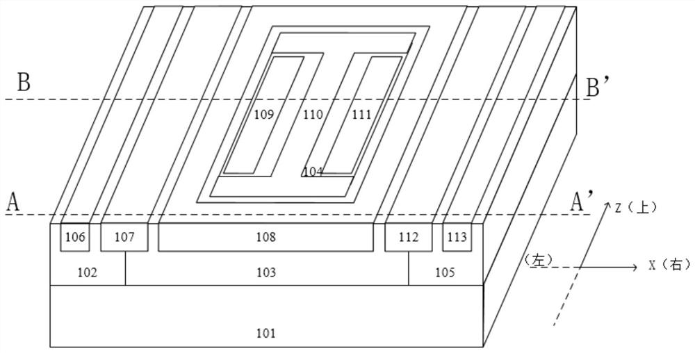
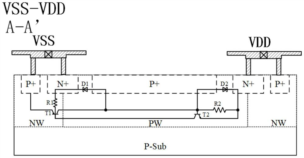
[0032] Such as figure 1As shown, a bidirectional voltage stabilized electrostatic surge full-chip protection integrated circuit includes a P-type substrate 101, and the upper surface of the P-type substrate 101 is respectively provided with a first P well 103, a first N well 102 and a second N well. Well 105, the left side of the first P well 103 is connected to the right side of the first N well 102, the left side of the first N well 102 is flush with the left side of the P-type substrate 101, the first N well 102 is provided with a first P+ implantation region 106, and the right side of the first P+ implantation region 106 is provided with a first N+ implantation region 107 at intervals, and the first N+ implantation region 107 is respectively on the first N well 102 and the first P well 103 ;
[0033] The right side of the first P well 103 is connected to the left side of the second N well 105, the right side of the second N well 105 is flush with the right side of the P-t...
Embodiment 2
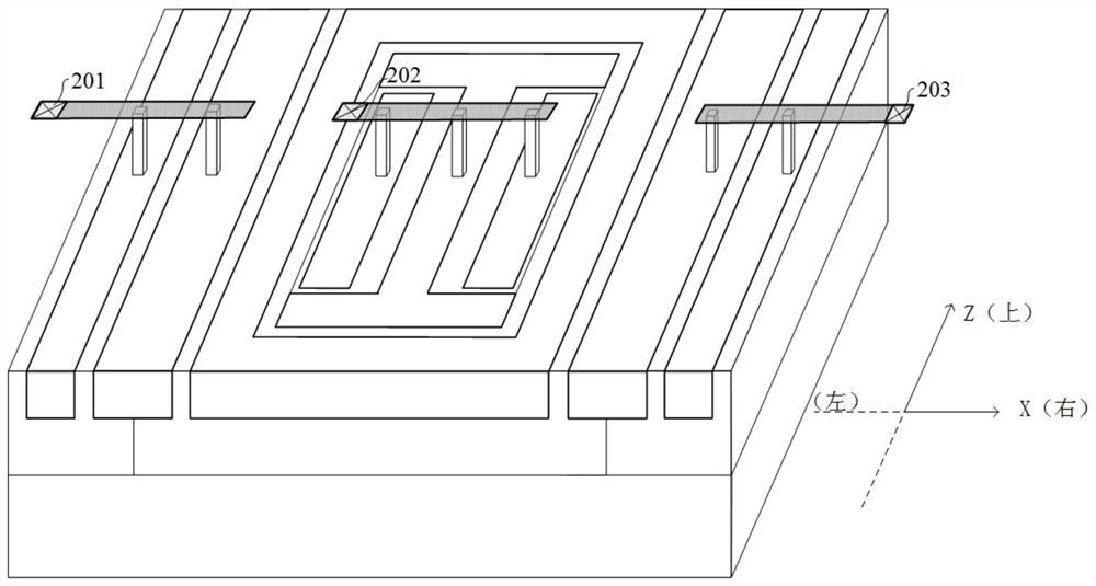
[0052] Such as Figure 5 As shown, in this embodiment, the P-type substrate 101, the first P well 103, the first N well 102, the second N well 105, the first P+ implantation region 106, the first N+ implantation region 107, and the fifth P+ implantation region 113 , the structural relationship between the third N+ implantation region 112 and the second P+ implantation ring 108 refers to Embodiment 1.
[0053] Specifically, the third P well 103 is respectively provided with a third N well 104 and a first N+ injection ring 301 in the second P+ injection ring 108, and the first N+ injection ring 301 is respectively provided in the third N well 104 and the first P well 103, the third N well 104 is provided with a sixth P+ implantation region 302 in the first N+ implantation ring 301, the distance between the left side of the sixth P+ implantation region 302 and the first N+ implantation ring 301 and the sixth P+ implantation region The distance between the right side of 302 and t...
Embodiment 3
[0056] Such as Figure 6 As shown, in this embodiment, the P-type substrate 101, the first P well 103, the first N well 102, the second N well 105, the first P+ implantation region 106, the first N+ implantation region 107, and the fifth P+ implantation region 113 , the structural relationship between the third N+ implantation region 112 and the second P+ implantation ring 108 refers to Embodiment 1.
[0057] Specifically, the third P well 103 is provided with a third N well 104 in the second P+ implantation ring 108, and the third N well 104 is provided with a Japanese-shaped fourth N+ implantation region in the second P+ implantation ring 108 along the lateral direction. 401, the four sides of the fourth N+ implantation region 401 are respectively on the third P well 103 and the third N well 104, the left N+ ring and the right N+ ring of the fourth N+ implantation region 401 are arranged symmetrically, and the third N well 104 is on A seventh P+ implantation region 402 is a...
PUM
 Abstract
Description
Claims
Application Information
 - R&D Engineer
- R&D Manager
- IP Professional
- Industry Leading Data Capabilities
- Powerful AI technology
- Patent DNA Extraction
Browse by: Latest US Patents, China's latest patents, Technical Efficacy Thesaurus, Application Domain, Technology Topic, Popular Technical Reports.
© 2024 PatSnap. All rights reserved.Legal|Privacy policy|Modern Slavery Act Transparency Statement|Sitemap|About US| Contact US: help@patsnap.com