Electrochromic device capable of being cut at will and application
A technology of electrochromic devices and electrochromic layers, which is applied in the directions of instruments, optics, nonlinear optics, etc., can solve the problems of high production costs, increased manufacturing costs of electrochromic film devices, limitations of electrochromic devices, etc.
- Summary
- Abstract
- Description
- Claims
- Application Information
AI Technical Summary
Problems solved by technology
Method used
Image

Examples
Embodiment 1
[0054] An electrochromic device that can be tailored arbitrarily is prepared by the following method:
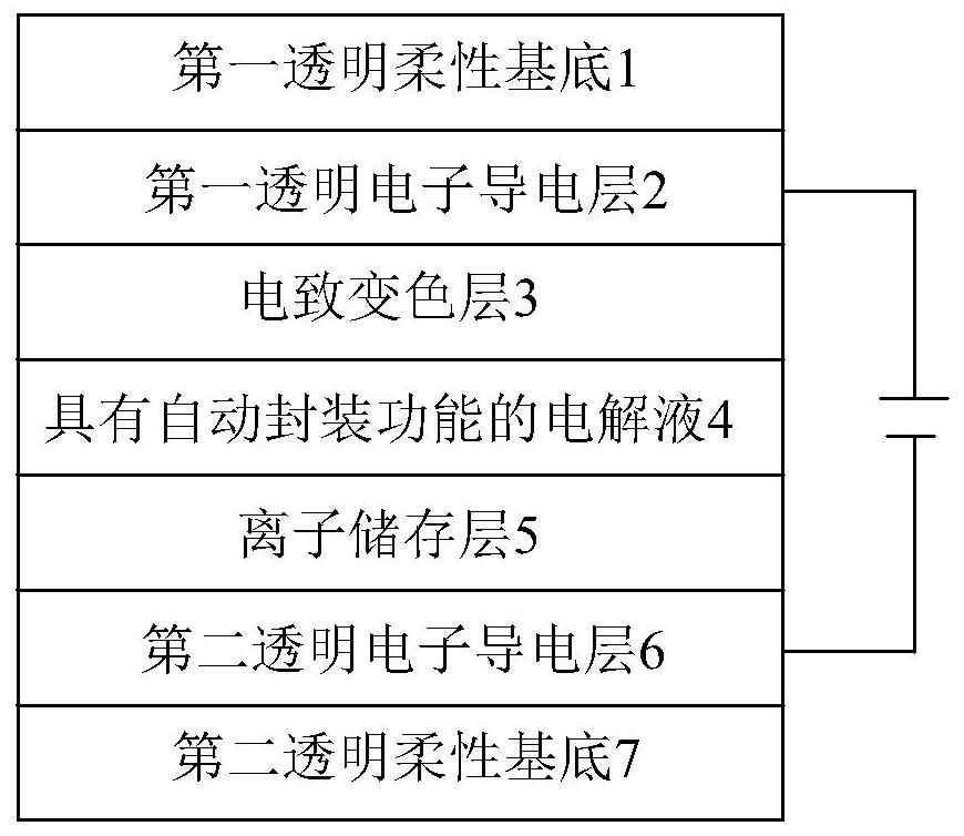
[0055] Both the first transparent flexible substrate and the second transparent flexible substrate are made of PET with a thickness of 175 μm, and the materials of the first transparent electronic conductive layer and the second transparent conductive layer are both made of ITO, the thickness of the ITO layer is 100 nm, and the square resistance is 10Ω / □.
[0056] The electrochromic layer is selected from electroplated Prussian Blue (Prussian Blue, PB), and its preparation process is: the first transparent flexible substrate and the first transparent conductive layer are formed as a whole (that is, the first PET-ITO substrate (PET-ITO substrate can be The ITO layer is magnetron sputtered on the PET substrate, or the prepared PET-ITO substrate can also be purchased directly)) and ultrasonically cleaned with acetone, deionized water, and ethanol for 5 minutes for later use. ...
Embodiment 2
[0061] An electrochromic device that can be tailored arbitrarily is prepared by the following method:
[0062] The first transparent flexible substrate and the second transparent flexible substrate are made of PET with a thickness of 175 μm, the first transparent electronic conductive layer and the second transparent conductive layer are made of ITO, the thickness of the ITO layer is 100nm, and the square resistance is 10Ω / □ .
[0063] The electrochromic layer is made of electroplated PANI (polyaniline), and its preparation process is as follows: the PET-ITO substrate is ultrasonically cleaned with acetone, deionized water, and ethanol for 5 minutes respectively. Configure the plating solution, which includes 100mM aniline and 1M H 2 SO 4 . Use the PET-ITO substrate as the working electrode, a 1 square centimeter platinum sheet as the counter electrode, and Ag / AgCl as the reference electrode, apply +2.0v at room temperature, electroplate for 45s, gently rinse the film with ...
Embodiment 3
[0068] An electrochromic device that can be tailored arbitrarily is prepared by the following method:
[0069] Both the first transparent flexible substrate and the second transparent flexible substrate are made of PET with a thickness of 175 μm, the materials of the first transparent electronic conductive layer and the second transparent conductive layer are made of ITO, the thickness of the ITO layer is 100 nm, and the square resistance is 10Ω / □ .
[0070] Magnetron sputtered WO 3 , the preparation process is as follows: put the PET-ITO substrate into the loading chamber of the magnetron sputtering equipment, use ions to bombard the transparent film substrate to eliminate static electricity, vacuumize after sealing, and then transport the PET-ITO substrate to The sputtering chamber is deposited by magnetron sputtering to obtain WO 3 layer as an electronic color-changing layer; the target used in magnetron sputtering equipment is tungsten target, DC / RF power supply is used ...
PUM
| Property | Measurement | Unit |
|---|---|---|
| Thickness | aaaaa | aaaaa |
| Thickness | aaaaa | aaaaa |
| Square resistance | aaaaa | aaaaa |
Abstract
Description
Claims
Application Information
 - R&D
- Intellectual Property
- Life Sciences
- Materials
- Tech Scout
- Unparalleled Data Quality
- Higher Quality Content
- 60% Fewer Hallucinations
Browse by: Latest US Patents, China's latest patents, Technical Efficacy Thesaurus, Application Domain, Technology Topic, Popular Technical Reports.
© 2025 PatSnap. All rights reserved.Legal|Privacy policy|Modern Slavery Act Transparency Statement|Sitemap|About US| Contact US: help@patsnap.com