Silk-screen printing welding method of dielectric device and dielectric device

A technology of screen printing and welding method, which is applied in the direction of printing and printing devices, which can solve problems such as increasing the number of silver burning times, increasing insertion loss, and burrs on etching rings, so as to improve product performance and reliability and reduce manufacturing processes , Reduce the effect of etching process

Inactive Publication Date: 2021-03-12
无锡市高宇晟新材料科技有限公司
View PDF7 Cites 0 Cited by
  • Summary
  • Abstract
  • Description
  • Claims
  • Application Information

AI Technical Summary

Problems solved by technology

The disadvantages of this process are: first, an additional laser etching process is added, which will damage the surface of the dielectric block, and burrs and other undesirable phenomena will appear on the edge of the etching ring, which will increase the insertion loss of the product; second, the process requires Laser etching is performed on the metallized silver-burned product. The etched product needs to print the silver layer welding point, and then perform the silver layer infiltration welding at high temperature, which will increase the number of times of silver burning and the multiple sintering of the metal paste layer It will cause the glass phase to float up, thereby increasing the insertion loss and affecting the electrical performance of the product
[0004] In summary, there are obviously inconveniences and defects in the actual use of the existing technology, so it is necessary to improve

Method used


Image

  • Silk-screen printing welding method of dielectric device and dielectric device
  • Silk-screen printing welding method of dielectric device and dielectric device
  • Silk-screen printing welding method of dielectric device and dielectric device

Examples


Embodiment Construction

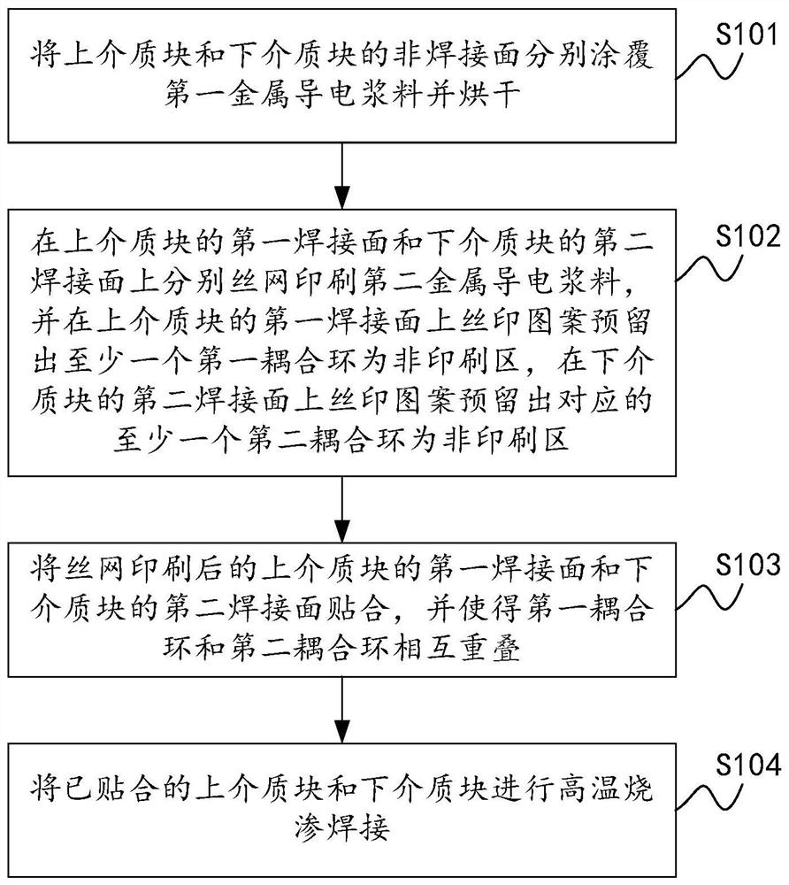
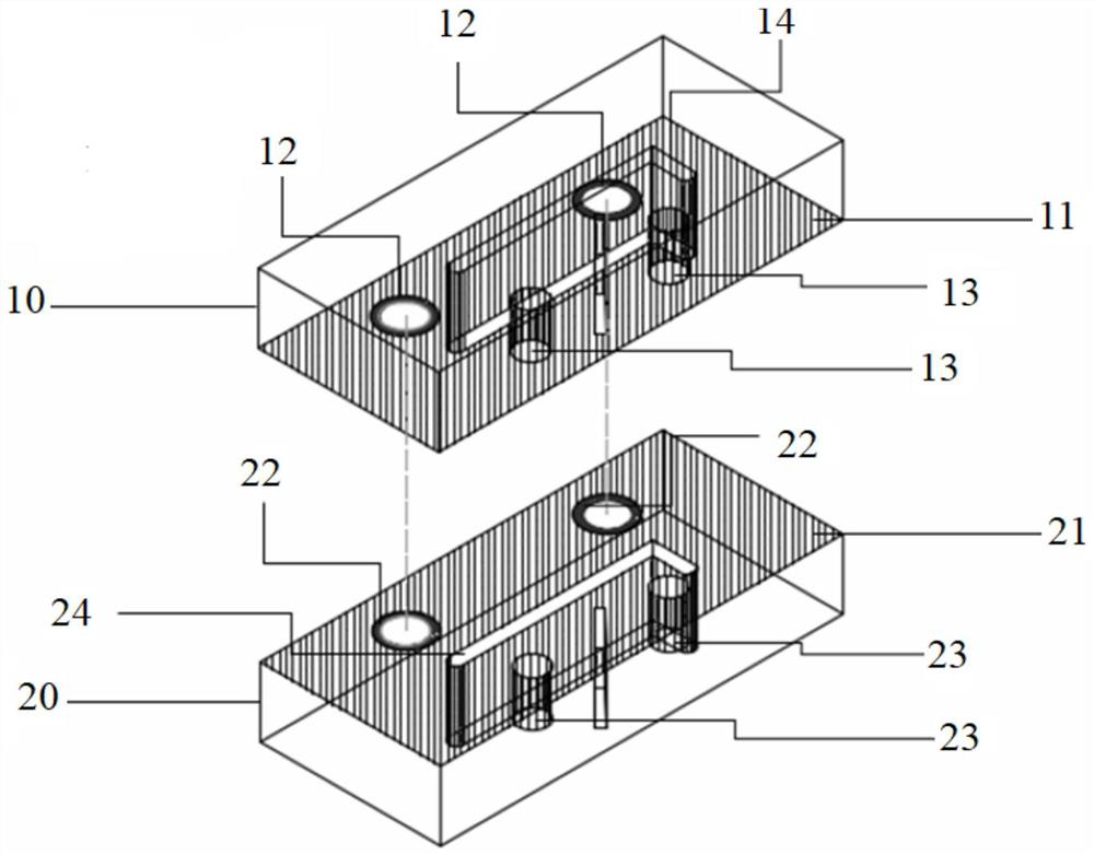
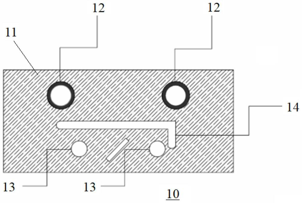
[0035] In order to make the object, technical solution and advantages of the present invention clearer, the present invention will be further described in detail below in conjunction with the accompanying drawings and embodiments. It should be understood that the specific embodiments described here are only used to explain the present invention, not to limit the present invention.

[0036] It should be noted that references in this specification to "one embodiment", "embodiment", "example embodiment" and the like mean that the described embodiment may include specific features, structures or characteristics, but not every Embodiments must include those specific features, structures or characteristics. Furthermore, such expressions are not referring to the same embodiment. Further, when specific features, structures or characteristics are described in conjunction with an embodiment, whether or not there is an explicit description, it has been indicated that it is within the kn...


PUM

PropertyMeasurementUnit
quality factoraaaaaaaaaa
viscosityaaaaaaaaaa
temperatureaaaaaaaaaa

Abstract

The invention provides a silk-screen printing welding method of a dielectric device. The silk-screen printing welding method comprises the following steps: respectively coating non-welding surfaces ofan upper dielectric block and a lower dielectric block with first metal conductive paste and drying; performing silk-screen printing of second metal conductive paste on the welding surfaces of the upper dielectric block and the lower dielectric block respectively, and performing silk-screen printing of patterns on the welding surfaces of the upper dielectric block and the lower dielectric block respectively to reserve at least one corresponding coupling ring as a non-printing area; fitting the welding surfaces of the upper dielectric block and the lower dielectric block after silk-screen printing, and enabling the coupling rings of the upper dielectric block and the lower dielectric block to be overlapped with each other; and carrying out high-temperature sintering infiltration welding onthe upper dielectric block and the lower dielectric block which are attached to each other. Correspondingly, the invention further provides the dielectric device manufactured through the silk-screenprinting welding method of the dielectric device. Therefore, the performance and reliability of the product can be improved, and the production efficiency of the product is improved.

Description

technical field [0001] The invention relates to the technical field of dielectric devices for wireless communication, in particular to a screen printing welding method for a dielectric device and the dielectric device. Background technique [0002] The miniaturization of 5G communication base stations has promoted the development of microwave dielectric ceramic technology, and made dielectric devices such as dielectric filters, dielectric combiners, dielectric resonators, and dielectric duplexers and multiplexers become hot spots in current development. Compared with the traditional metal cavity, the dielectric device has the advantages of high frequency selectivity, good filtering performance, high quality factor, low insertion loss, and low temperature drift coefficient. [0003] The manufacturing process of the existing dielectric device is: spray silver on the surface of the dielectric block and dry it, then infiltrate the silver layer at high temperature, laser etch the...

Claims


Application Information

Patent Timeline
Patent Type & Authority Applications(China)
IPC IPC(8): C04B37/00B41M1/12
CPCC04B37/006B41M1/12C04B2237/125C04B2237/55
Inventor 黄名政黄庆焕徐海新
Owner 无锡市高宇晟新材料科技有限公司
Why Eureka
Try Eureka