Functional substrate, liquid crystal display panel and display
A liquid crystal display panel and substrate technology, which is applied to instruments, nonlinear optics, optics, etc., can solve the problems of insufficient shading effect and decreased display contrast, and achieve the effect of increasing adhesion, ensuring shading effect, and avoiding the decrease of display contrast.
- Summary
- Abstract
- Description
- Claims
- Application Information
AI Technical Summary
Problems solved by technology
Method used
Image

Examples
Embodiment 1
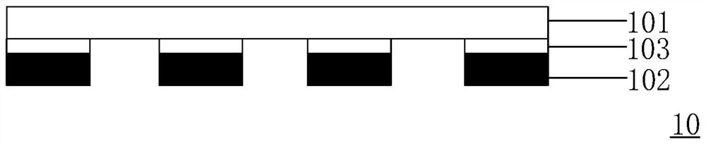
[0033] Usually, the liquid crystal display panel consists of a color filter substrate (CF, Color Filter), a thin film transistor substrate (TFT, ThinFilm Transistor), a liquid crystal (LC, Liquid Crystal) sandwiched between the color filter substrate and the thin film transistor substrate, and a sealant frame (Sealant )composition. Among them, the thickness of the liquid crystal layer, that is, the thickness of the cell (Cell Gap) is mainly controlled by the height of the spacer (Post Spacer, PS) arranged between the array substrate and the color filter substrate, and the thickness of the liquid crystal layer has a great influence on the structural parameters of the liquid crystal display device. and display quality have an important impact, usually the spacers are formed on the side of the color filter substrate. The color filter substrate generally includes a substrate, a light-shielding unit (such as a black matrix) formed on the substrate, and a color filter layer. The lig...
Embodiment 2
[0037] In order to better describe the functional substrate of the first embodiment, this embodiment specifically describes the specific structure of the liquid crystal substrate on the basis of the foregoing embodiments.
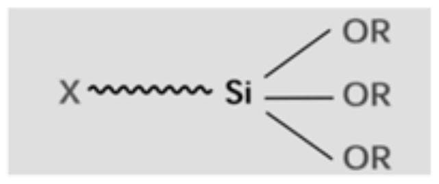
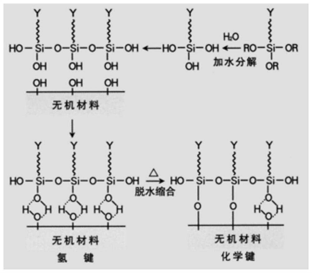
[0038] In the current manufacturing process of color substrates, the light-shielding unit (such as black matrix) is generally in direct contact with the smooth glass substrate by coating. During the peeling test in the panel reliability test, the black matrix and the glass on which it is located The substrates will be separated under the peeling force, which indicates that the interface adhesion between the black matrix and the glass substrate on which it is located is insufficient. Therefore, in order to solve the problem that the black matrix is easy to peel off from the glass substrate, please refer to figure 2 In this embodiment, the coupling layer 103 is selected as a silane coupling agent (Y-R-Si(OR) 3), and Y-R- is recorded as X, the silaneoxy gr...
Embodiment 3
[0046] An embodiment of the present invention further provides a liquid crystal display panel, and the liquid crystal display panel of this embodiment will be described in detail on the basis of the foregoing embodiments.
[0047] See Figure 5 , Figure 5 It is a schematic structural diagram of a liquid crystal display panel provided by an embodiment of the present invention. The liquid crystal display panel includes a functional substrate 10, a second substrate 20, and a liquid crystal layer 30, wherein the functional substrate 10 and the second substrate 20 are oppositely arranged, and the liquid crystal layer 30 is arranged between the functional substrate 10 and the second substrate 20, that is, the first A substrate 101 is disposed opposite to the second substrate 20 , and the liquid crystal layer 30 and the light-shielding unit 102 are disposed between the functional substrate 10 and the second substrate 20 . The TFT-LCD panel can be regarded as a layer of liquid crys...
PUM
| Property | Measurement | Unit |
|---|---|---|
| thickness | aaaaa | aaaaa |
Abstract
Description
Claims
Application Information
 - R&D
- Intellectual Property
- Life Sciences
- Materials
- Tech Scout
- Unparalleled Data Quality
- Higher Quality Content
- 60% Fewer Hallucinations
Browse by: Latest US Patents, China's latest patents, Technical Efficacy Thesaurus, Application Domain, Technology Topic, Popular Technical Reports.
© 2025 PatSnap. All rights reserved.Legal|Privacy policy|Modern Slavery Act Transparency Statement|Sitemap|About US| Contact US: help@patsnap.com