Method for preparing large-area single crystal copper foil
A large-area, copper foil technology, applied in the field of materials, can solve problems such as easy adhesion and affect the effect, achieve excellent lubricity, reduce interaction, and maintain regular and smooth effects
- Summary
- Abstract
- Description
- Claims
- Application Information
AI Technical Summary
Problems solved by technology
Method used
Image
Examples
Embodiment 1
[0056] In this example, the carrier used had a rectangular graphite plate similar to the rectangular quartz plate used in Comparative Example 1. The structure of the annealing device mainly includes the plate body, pillars and grooves. The plate body is the part of the carrier that actually carries the copper foil, and the pillars and grooves mainly play the role of interlayer support and positioning. In the process of carrier stacking, except for the first layer, the pillars of each layer of rectangular quartz plates are closely attached to the grooves of the upper layer, which creates a suitable interlayer spacing for annealing while limiting the displacement between layers in the horizontal direction. A carrier batch with a monolithic structure is formed, enabling batch fabrication in a single annealing process.
[0057] In this example, the conditions and steps of annealing are the same as in Comparative Example 1. The annealing furnace used is a three-temperature zone ann...
Embodiment 2
[0066] In the present embodiment, the carrier used is a wave-shaped graphite plate, the length of the wave-shaped graphite plate is 330mm, the diameter of each wave in the wave shape is 20mm, and the thickness is 5mm. Its shape is as follows: Figure 3a shown. The structure of the annealing apparatus is the same as in Embodiment 1.
[0067] The annealing conditions and process steps used are consistent with those in Example 1.
[0068] The single-crystallized copper foil obtained in this embodiment has a variety of crystal planes, and the obtained results are as follows: Figure 3a-Figure 3d shown, where Figure 3a showing the top and left side views of the corrugated board, and schematic diagrams of the placement of the copper foil on the corrugated board at different b, c and d positions, Figure 3b , Figure 3c with Figure 3d respectively in Figure 3a EBSD analysis patterns of single crystal copper foils sampled at different b, c and d positions. It can be seen tha...
Embodiment 3
[0070] In this embodiment, the carrier used is a stepped graphite plate, the length of the stepped graphite plate is 304.5mm, the width is 75.5mm, the thickness is 3mm, and the step spacing is 5mm. Its shape is as follows: Figure 4a shown. The structure of the annealing apparatus is the same as in Embodiment 1.
[0071] The annealing conditions and process steps used are consistent with those in Example 1.
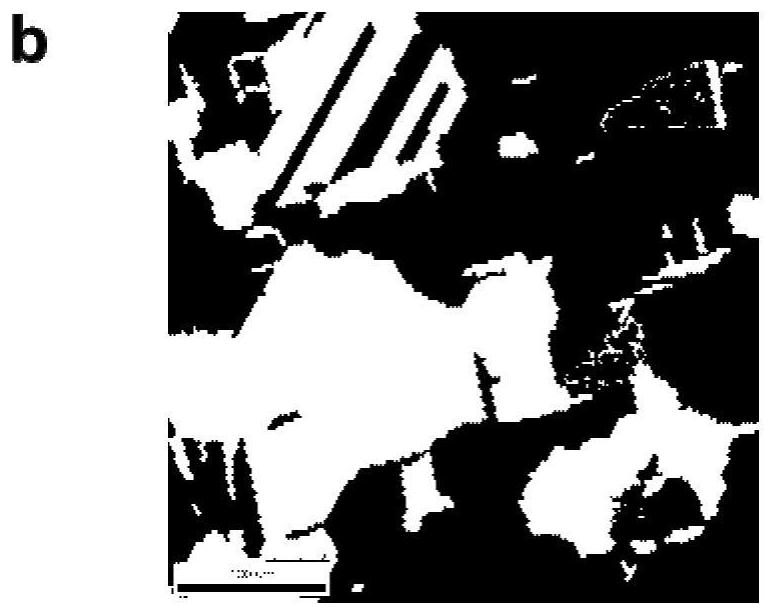
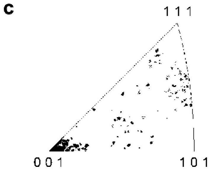
[0072] In the single-crystallized copper foil obtained in this example, the crystal plane at the step is prone to abrupt changes due to stress, thereby forming a high-index crystal plane. The obtained results are as follows Figures 4a-4c shown, where Figure 4a Showing top and left side views of a stepped graphite plate and a schematic diagram of copper foil placement on the stepped plate, Figure 4b with 4c It is the EBSD analysis pattern of single crystal copper obtained by sampling. It can be seen that under the stress condition of the stepped carrier, various cr...
PUM
| Property | Measurement | Unit |
|---|---|---|
| Length | aaaaa | aaaaa |
| Thickness | aaaaa | aaaaa |
| Length | aaaaa | aaaaa |
Abstract
Description
Claims
Application Information
 - R&D
- Intellectual Property
- Life Sciences
- Materials
- Tech Scout
- Unparalleled Data Quality
- Higher Quality Content
- 60% Fewer Hallucinations
Browse by: Latest US Patents, China's latest patents, Technical Efficacy Thesaurus, Application Domain, Technology Topic, Popular Technical Reports.
© 2025 PatSnap. All rights reserved.Legal|Privacy policy|Modern Slavery Act Transparency Statement|Sitemap|About US| Contact US: help@patsnap.com


