Metal TCO laminated film and preparation method thereof and HIT solar cell
A technology of solar cells and metal film layers, applied in the field of solar cells, can solve the problems of low power generation efficiency of solar cell modules or products, poor effective transmittance of TCO thin films of solar cells, etc.
- Summary
- Abstract
- Description
- Claims
- Application Information
AI Technical Summary
Problems solved by technology
Method used
Image

Examples
preparation example Construction
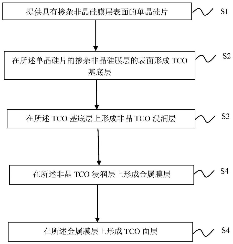
[0030] In some embodiments, a method for preparing the metal TCO laminated film is provided, comprising the following steps, such as image 3 Shown:
[0031] S1: Provide a single crystal silicon wafer with a doped amorphous silicon film surface;
[0032] S2: forming a TCO base layer on the surface of the doped amorphous silicon film layer of the single crystal silicon wafer;
[0033] S3: forming an amorphous TCO wetting layer on the TCO base layer;
[0034] S4: forming a metal film layer on the amorphous TCO wetting layer;
[0035] S5: forming a TCO surface layer on the metal film layer.
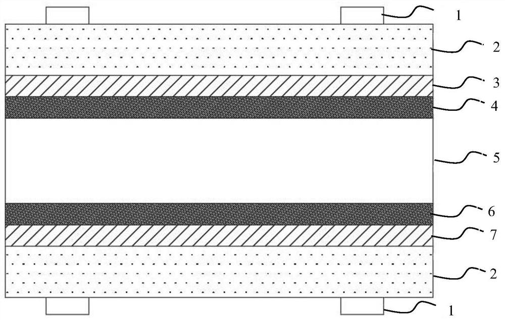
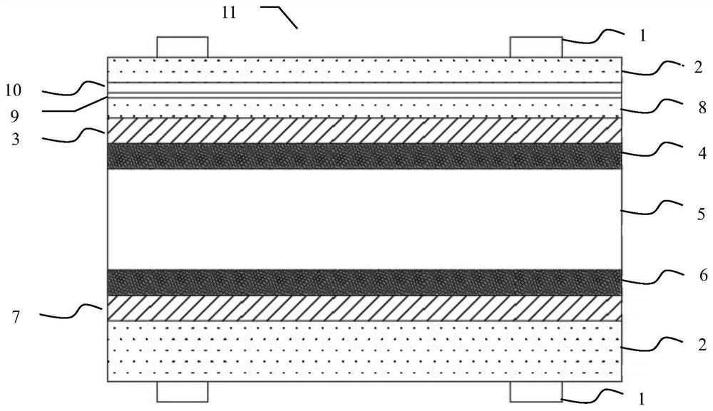
[0036] Specifically, the monocrystalline silicon wafer with a doped amorphous silicon film layer includes a silicon wafer provided with an N-type amorphous silicon layer or a P-type amorphous silicon layer on the surface of a single crystal silicon wafer, or a single crystal silicon wafer Single-crystal silicon wafers with an N-type amorphous silicon layer and a P-type amorphous silicon ...
Embodiment 1
[0054] S1: Provide a single crystal silicon wafer with an N-type doped amorphous silicon film on the surface, the thickness of the single crystal silicon wafer is 150 μm, and the resistivity is 10Ω·cm; the N-type doped amorphous silicon film layer of the single crystal silicon wafer is purged with nitrogen s surface;
[0055] S2: The magnetron sputtering chamber is evacuated, and the pressure of the chamber is evacuated to 5Pa; start and perform pre-sputtering, the pre-sputtering power is 140w, and the pre-sputtering time is 5min; the monocrystalline silicon wafer is preheated, and the heating temperature To 200°C; sputtering coating TCO base layer, sputtering power 140w, sputtering pressure 1.0Pa; sputtering time 5min, annealing treatment, on the surface of N-type doped amorphous silicon film layer of single crystal silicon wafer Form the TCO base layer;
[0056] S3: continue to sputter the amorphous TCO wetting layer, keep the same sputtering conditions, and sputter for 1 m...
Embodiment 2
[0061] S1: Provide a single crystal silicon wafer with an N-type doped amorphous silicon film on the surface, the thickness of the single crystal silicon wafer is 130 μm, and the resistivity is 5Ω·cm; the N-type doped amorphous silicon film layer of the single crystal silicon wafer is purged with nitrogen s surface;
[0062] S2: The magnetron sputtering chamber is evacuated, and the pressure of the chamber is evacuated to 3Pa; start and perform pre-sputtering, the pre-sputtering power is 100w, and the pre-sputtering time is 4min; the monocrystalline silicon wafer is preheated, and the heating temperature is To 180°C; sputtering coating TCO base layer, sputtering power 100w, sputtering pressure 1.0Pa; sputtering time 4min, annealing treatment, on the surface of N-type doped amorphous silicon film layer of single crystal silicon wafer Form the TCO base layer;
[0063] S3: continue to sputter the amorphous TCO wetting layer, keep the same sputtering conditions, and sputter for 1...
PUM
| Property | Measurement | Unit |
|---|---|---|
| thickness | aaaaa | aaaaa |
| thickness | aaaaa | aaaaa |
| electron work function | aaaaa | aaaaa |
Abstract
Description
Claims
Application Information
 - Generate Ideas
- Intellectual Property
- Life Sciences
- Materials
- Tech Scout
- Unparalleled Data Quality
- Higher Quality Content
- 60% Fewer Hallucinations
Browse by: Latest US Patents, China's latest patents, Technical Efficacy Thesaurus, Application Domain, Technology Topic, Popular Technical Reports.
© 2025 PatSnap. All rights reserved.Legal|Privacy policy|Modern Slavery Act Transparency Statement|Sitemap|About US| Contact US: help@patsnap.com