SiC MOSFET packaging structure optimization design method, medium and equipment

A packaging structure and optimization design technology, applied in design optimization/simulation, computer-aided design, calculation, etc., can solve problems such as accelerated wire peeling, solder cracks, etc., to achieve high design efficiency, improve device structure, and improve the effect of analysis efficiency

Active Publication Date: 2021-01-01
FUDAN UNIV
View PDF4 Cites 6 Cited by
  • Summary
  • Abstract
  • Description
  • Claims
  • Application Information

AI Technical Summary

Problems solved by technology

In addition, as the temperature magnitude increases, prolonged thermal cycling can easily accelerate wear processes such as wire stripping, solder cracking, etc.

Method used


Image

  • SiC MOSFET packaging structure optimization design method, medium and equipment
  • SiC MOSFET packaging structure optimization design method, medium and equipment
  • SiC MOSFET packaging structure optimization design method, medium and equipment

Examples


Embodiment 1

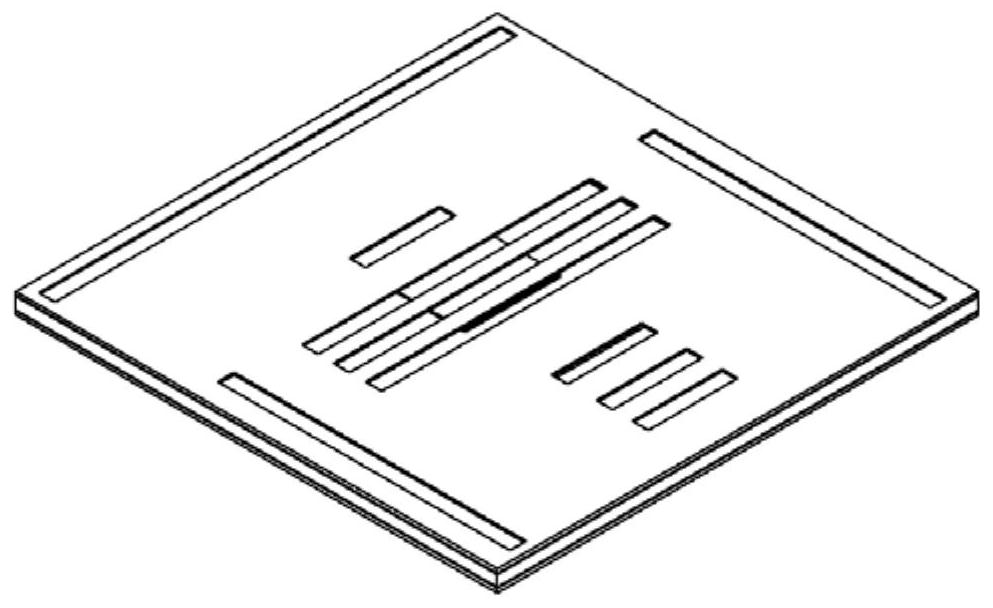
[0035] This embodiment provides a method for optimizing the packaging structure of an embedded fan-out SiC MOSFET, which is mainly applied to occasions for optimizing the reliability of power devices and modules. This method uses the response surface method to optimize the design and analysis of the simulation. Based on the finite element simulation analysis, the maximum heat dissipation temperature of the redistribution layer (RDL) in the SiC MOSFET in the steady state heat dissipation and the maximum stress after the temperature cycle simulation are calculated. The mathematical model between the distribution of the chip and the heat dissipation temperature and the maximum stress, so as to find out the optimal chip distribution mode for heat dissipation and stress, so as to achieve the purpose of optimization.

[0036] Such as figure 1 As shown, the method includes the following steps:

[0037] Step 1: Establish a three-dimensional model of the SiC MOSFET device, and determi...

Embodiment 2

[0057] This embodiment provides a computer-readable storage medium, on which a computer program is stored, and when the computer program is executed by a processor, the steps of the method for optimizing the packaging structure of an embedded fan-out SiC MOSFET as described in Embodiment 1 are realized. .

Embodiment 3

[0059] The present invention also provides an electronic device, comprising a processor and a memory storing processor-executable instructions, wherein the processor is coupled to the memory for reading program instructions stored in the memory, and in response, The steps in the method for optimizing the packaging structure of the embedded fan-out SiC MOSFET described in Embodiment 1 are performed.


PUM


Abstract

The invention relates to an embedded fan-out type SiC MOSFET packaging structure optimization design method, a medium and equipment, and the method comprises the steps: building a three-dimensional model of a SiC MOSFET device, determining a feasible region of chip distribution, carrying out the simulation parameter design based on the feasible region through employing a response surface method, and carrying out the finite element simulation based on simulation parameters; constructing a mathematical model between the distribution condition of the chips and the maximum heat dissipation temperature and the maximum stress according to a simulation result, thereby obtaining a chip distribution mode with optimal heat dissipation and stress, and realizing optimal design of the packaging structure. Compared with the prior art, the method has the advantages of high analysis efficiency, high optimization accuracy and the like.

Description

technical field [0001] The invention belongs to the field of reliability optimization of semiconductor devices, and relates to power electronic devices, finite element analysis, and response surface experiment optimization design, and in particular to a SiC MOSFET packaging structure optimization design method, medium and equipment. Background technique [0002] Compared with Si chips, SiC chips can achieve higher withstand voltage and lower loss with a smaller volume, which brings more convenience to the development and design of traction conversion systems and power transmission systems. In addition, SiC chips have lower output capacitance and gate charge. The characteristics of high switching speed, low switching loss and high switching frequency can improve the power density and efficiency of the power module. At higher temperature, the switching loss of Si IGBT will increase significantly, while the switching loss of SiC MOSFET does not change much with temperature. H...

Claims


Application Information

Patent Timeline
Patent Type & Authority Applications(China)
IPC IPC(8): G06F30/23G06F30/392G06F30/398G06F111/10G06F113/18G06F119/08G06F119/14
CPCG06F30/23G06F30/392G06F30/398G06F2113/18G06F2111/10G06F2119/08G06F2119/14
Inventor 樊嘉杰钱弈晨侯峰泽刘盼张国旗
Owner FUDAN UNIV
Why Eureka
Try Eureka