CMOS holographic microscopic imaging device and method applied to cell segmentation

An imaging device and holographic microscopy technology, applied in the field of microscope imaging, can solve the problems of weak absorption in the visible light band, inconvenient integration and commercialization, and the influence of sample activity, so as to improve the level of medical detection technology, improve the limit resolution, simple method effect

Active Publication Date: 2020-12-25
SHANDONG IND TECH RES INST OF ZHEJIANG UNIV
View PDF11 Cites 0 Cited by
  • Summary
  • Abstract
  • Description
  • Claims
  • Application Information

AI Technical Summary

Problems solved by technology

[0005] In terms of improving resolution, the current pixel super-resolution method of super-resolution requires a high-precision translation stage to move the sample by a sub-pixel displacement distance, which will bring higher costs and burdens to the experiment, and is not easy to integrate and commercialize.
The method of super-resolution enhancement using artificial intelligence may distort the image, and at the same time require extremely high computing costs, which will also bring higher costs and burdens to the laboratory
[0006] For lensless microscopic imaging, the existing super-resolution methods are difficult to meet the current needs of non-invasive imaging in the biomedical field, that is, in the field of biological imaging, when biological samples are marked by staining and other means, the activity of the sample will be generated. influences
However, for most unstained biological cell samples, due to their weak absorption in the visible light band, they cannot be directly collected by the camera, so they must be imaged with the help of phase information

Method used


Image

  • CMOS holographic microscopic imaging device and method applied to cell segmentation
  • CMOS holographic microscopic imaging device and method applied to cell segmentation
  • CMOS holographic microscopic imaging device and method applied to cell segmentation

Examples


Embodiment 1

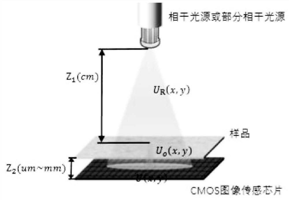
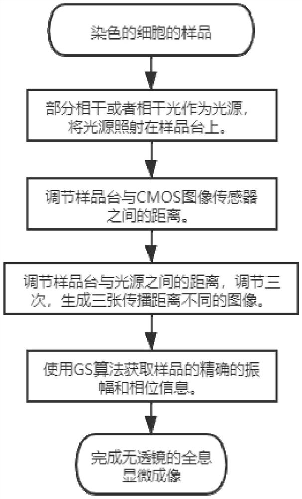
[0063] Embodiment one, such as figure 2 As shown, the CMOS holographic microscopic imaging method applied to cell segmentation comprises the following steps:

[0064] S1. Place the imaging sample on the sample stage, and turn on the light source.

[0065] S2. Adjust the distance between the sample stage and the CMOS image sensor chip so that the axial distance Z between the light source and the sample stage 1 Greater than the axial distance Z between the sample stage and the CMOS image sensor chip 2 At this time, the coherent light emitted by the light source and the object wave light formed by the scattering of the coherent light on the surface of the imaging sample are superimposed on the front of the CMOS image sensor chip to generate interference.

[0066] S3. Change the axial distance Z between the light source and the sample stage in turn 1 Three times, to obtain three different axial distances Z 1 The image (20MM, 18mm, 16mm) describes the relationship between the ...


PUM

PropertyMeasurementUnit
Sizeaaaaaaaaaa

Abstract

The invention belongs to the technical field of microscope imaging, and particularly relates to a CMOS holographic microscopic imaging device and method applied to cell segmentation. The imaging device comprises a light source, a sample table and a CMOS image sensing chip, wherein the light source is used for emitting illumination light and is arranged on an optical axis of the imaging device, andthe illumination light is a coherent light source or a partially coherent light source; the sample table is used for placing an imaging sample; and the CMOS image sensing chip is electrically connected with a computer. On the basis of a traditional lensless microscopy technology, light intensity of three images with different vertical axis distances is calculated by using a light intensity transmission amplifier, approximate phase distribution information of an intermediate image is obtained, multiple iterations are carried out in combination with a GS algorithm to obtain accurate jolt degreeand phase information of a sample image, finally, the CMOS holographic microscopic imaging device and method applied to cell segmentation can improve the lensless field of view and the system limit resolution.

Description

technical field [0001] The invention belongs to the technical field of microscope imaging, and in particular relates to a CMOS holographic microscopic imaging device and method used in cell segmentation. Background technique [0002] Lensless holographic microscopic imaging is a digital microscopic technique that does not require a lens for imaging. Based on the principle of Gabor coaxial holography, it uses an area array detector to collect the original hologram, and then reconstructs the sample through digital image processing technology, so as to realize digital microscopic imaging. The resolution of traditional lensless technology reproduction results is limited by the pixel size of the photodetector, and its resolution is close to the pixel size. Similarly, due to the sensor manufacturing process level, the pixel size of the sensor cannot be infinitely small, so the imaging of the lensless microscope The resolution is often lower than the Nyquist sampling resolution de...

Claims


Application Information

Patent Timeline
IPC IPC(8): G02B21/00G02B21/34G02B21/36G01N15/14
CPCG02B21/0004G02B21/361G02B21/365G02B21/34G01N15/1434G01N2015/144G01N2015/1006
Inventor 吴健杜邦
Owner SHANDONG IND TECH RES INST OF ZHEJIANG UNIV
Why Eureka
Try Eureka