Plasmon absorber and preparation method thereof
A plasmon and absorber technology, applied in the field of optoelectronic devices, can solve the problems of poor chemical performance stability, difficult application of plasmon absorbers, poor optical absorption performance, etc.
- Summary
- Abstract
- Description
- Claims
- Application Information
AI Technical Summary
Problems solved by technology
Method used
Image
Examples
Embodiment 1
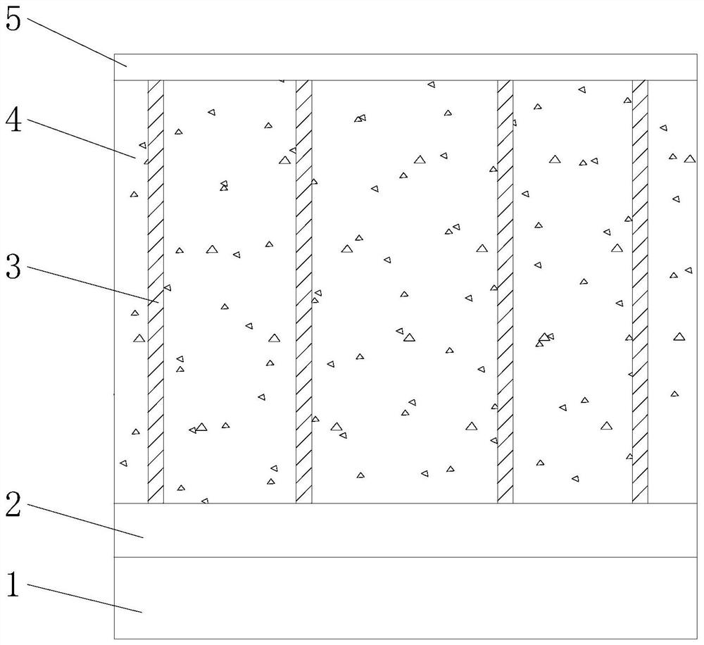
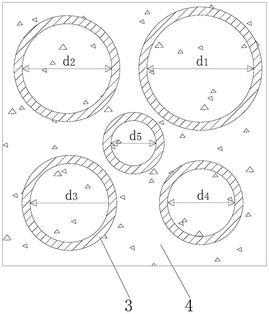
[0034] Such as figure 1 and figure 2 As shown, a plasmon absorber includes a periodic unit, the periodic unit is a base layer 1, a metal thin film layer 2 and a metal nanoring 3 from bottom to top, and the axis of the metal nanoring 3 perpendicular to the surface of the metal thin film layer 2, and the circumferential periphery of the metal nano-ring 3 is wrapped by a dielectric layer 4, and the inner region of the metal nano-ring 3 is filled by a dielectric layer 4, between the metal nano-ring 3 and The top of the dielectric layer 4 is covered with a protective layer 5 .
[0035] The base layer 1 and the metal thin film layer 2 are squares of the same size and overlapped and stacked together. The metal nano rings 3 are provided with five, one of which is arranged at the central area of the metal thin film layer 2, and the remaining four It is distributed around its circumference, specifically one is set at the four corners of the square metal thin film layer 2, the metal...
Embodiment 2
[0039]The difference from Embodiment 1 is that two metal nanorings 3 of the plasmonic absorber are arranged at intervals on the metal thin film layer 2, and a metal nanoring 3 is respectively arranged at the corners of the metal thin film layer 2. The inner diameters of the nano-rings 3 and the two metal nano-rings 3 are 400nm and 320nm respectively.
[0040] The wall thickness of the metal nanoring 3 is 20nm, the axial height of the metal nanoring 3 is 6 μm, and the side length of the base layer 1 and the metal thin film layer 2 is 900nm, and the thickness of the metal thin film layer 2 200nm, the thickness of the protective layer 5 is 40nm; the base layer 1 is made of alumina, the metal nanoring 3 and the metal thin film layer 2 are made of gold, and the dielectric layer 4 is made of gold. Made of alumina;
[0041] The above-mentioned plasmonic absorber can realize the absorption wavelength range from 300nm to 1500nm, and the average absorption efficiency can reach 94%.
Embodiment 3
[0043] The difference from Embodiment 1 is that the base layer is made of hafnium dioxide, and the dielectric layer 4 is made of hafnium dioxide.
[0044] There are five metal nano-rings 3, and the distribution is the same as in Embodiment 1. The inner diameters of the five metal nano-rings 3 can specifically be d 1 = 400nm, d 2 =360nm, d 3 =280nm,d 4 = 200nm, d 5 =120nm, and the wall thickness of the metal nanoring 3 is 20nm, the axial height of the metal nanoring 3 is 6 μm, and the side length of the base layer 1 and the metal thin film layer 2 is 900nm, the metal thin film The thickness of layer 2 is 200nm, and the thickness of described protective layer 5 is 40nm; Described metal nano ring 3, metal film layer 2 are made of gold;
[0045] The above-mentioned plasmonic absorber can realize the absorption wavelength range from 300nm to 1600nm, and the average absorption efficiency can reach 94%.
PUM
| Property | Measurement | Unit |
|---|---|---|
| thickness | aaaaa | aaaaa |
| height | aaaaa | aaaaa |
| thickness | aaaaa | aaaaa |
Abstract
Description
Claims
Application Information
 - Generate Ideas
- Intellectual Property
- Life Sciences
- Materials
- Tech Scout
- Unparalleled Data Quality
- Higher Quality Content
- 60% Fewer Hallucinations
Browse by: Latest US Patents, China's latest patents, Technical Efficacy Thesaurus, Application Domain, Technology Topic, Popular Technical Reports.
© 2025 PatSnap. All rights reserved.Legal|Privacy policy|Modern Slavery Act Transparency Statement|Sitemap|About US| Contact US: help@patsnap.com


