
Manufacturing method of memory device and capacitor thereof

A technology of a storage device and a manufacturing method, applied in the field of memory manufacturing, can solve the problems of limiting the integration degree and large area of ​​ferroelectric memory cells, and achieve the effects of improving the equivalent remanent polarization, high storage density, and easy integration

Active Publication Date: 2020-11-20
无锡舜铭存储科技有限公司
View PDF18 Cites 5 Cited by
  • Summary
  • Abstract
  • Description
  • Claims
  • Application Information

AI Technical Summary

Problems solved by technology

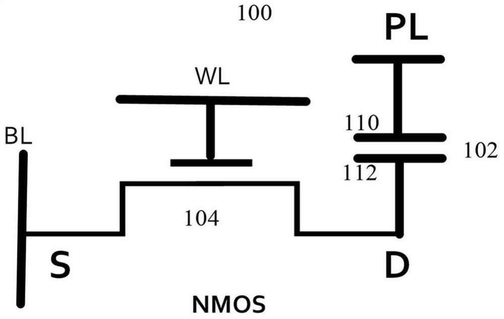
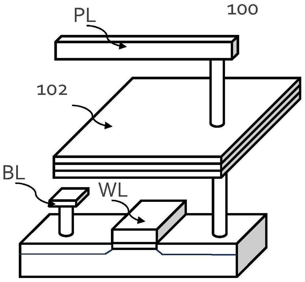
like figure 2 As shown, the existing planar ferroelectric capacitor 102 occupies a large area, which limits the integration of the ferroelectric memory cell

Method used


Image

  • Manufacturing method of memory device and capacitor thereof
  • Manufacturing method of memory device and capacitor thereof
  • Manufacturing method of memory device and capacitor thereof

Examples


Embodiment Construction

[0052] In the following description, the present invention is described with reference to various examples. One skilled in the art will recognize, however, that the various embodiments may be practiced without one or more of the specific details, or with other alternative and / or additional methods, materials, or components. In other instances, well-known structures, materials, or operations are not shown or described in detail so as not to obscure aspects of the various embodiments of the invention. Similarly, for purposes of explanation, specific quantities, materials and configurations are set forth in order to provide a thorough understanding of embodiments of the invention. However, the invention may be practiced without these specific details. Furthermore, it should be understood that the various embodiments shown in the drawings are illustrative representations and are not necessarily drawn to scale.

[0053] In this specification, reference to "one embodiment" or "the...


PUM


Abstract

The invention discloses a manufacturing method of a memory device. The manufacturing method comprises the following steps: providing a semiconductor substrate; forming a first interconnection structure, wherein the first interconnection structure comprises capacitor conductive columns, bit line conductive columns and a first dielectric layer between the conductive columns; forming a first bit lineconductive plug, wherein the first bit line conductive plug comprises metal conductive columns electrically connected with the bit line conductive columns and a second dielectric layer between the metal conductive columns; forming a third dielectric layer and a hard mask layer in sequence; patterning the hard mask layer through photoetching and etching processes, performing etching by taking thepatterned hard mask layer as a mask, forming deep holes in the second dielectric layer and the third dielectric layer, then removing the hard mask layer, and exposing the capacitor conductive columnsat the bottoms of the deep holes; forming a first electrode layer; forming a high-K ferroelectric oxide layer and a second electrode layer; and forming a metal interconnection, a board line and a bitline.

Description

technical field [0001] The invention relates to the field of manufacturing of memories. Specifically, the present invention relates to a manufacturing method of a storage device and a capacitor thereof. Background technique [0002] Ferroelectric memory is a non-volatile memory of a special process. When an electric field is applied to the ferrotransistor, the central atom follows the field and stops at the first low-energy state position, while when an electric field reversal is applied to the same ferrotransistor, the central atom moves in the crystal along the direction of the electric field and stops at The second lowest energy state. A large number of central atoms move and couple in the crystal unit cell to form ferroelectric domains, and the ferroelectric domains form polarized charges under the action of an electric field. The polarization charge formed by the ferroelectric domain reversal under the electric field is higher, and the polarization charge formed by t...

Claims


Application Information

Patent Timeline
Patent Type & Authority Applications(China)
IPC IPC(8): H01L27/11507H01L27/11514H10B53/30H10B53/20
CPCH10B53/20H10B53/30
Inventor 华文宇陶谦刘藩东夏季
Owner 无锡舜铭存储科技有限公司
Learn More