
Three-dimensional differential on-chip antenna based on silicon through hole

A technology of through-silicon vias and antennas, applied in the field of three-dimensional structure differential on-chip antennas, which can solve problems such as vertical interconnection, three-dimensional difficult-to-function chips, and large antenna volume

Active Publication Date: 2018-05-08
BEIJING INST OF REMOTE SENSING EQUIP
View PDF3 Cites 0 Cited by
  • Summary
  • Abstract
  • Description
  • Claims
  • Application Information

AI Technical Summary

Problems solved by technology

[0004] The purpose of the present invention is to provide a three-dimensional structural differential on-chip antenna based on through-silicon vias, which solves the problems of large volume, single-point feeding and difficulty in three-dimensional vertical interconnection with functional chips in existing planar on-chip antennas.

Method used


Image

  • Three-dimensional differential on-chip antenna based on silicon through hole
  • Three-dimensional differential on-chip antenna based on silicon through hole
  • Three-dimensional differential on-chip antenna based on silicon through hole

Examples


Embodiment Construction

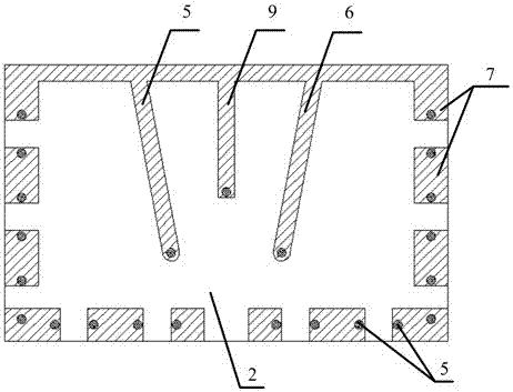
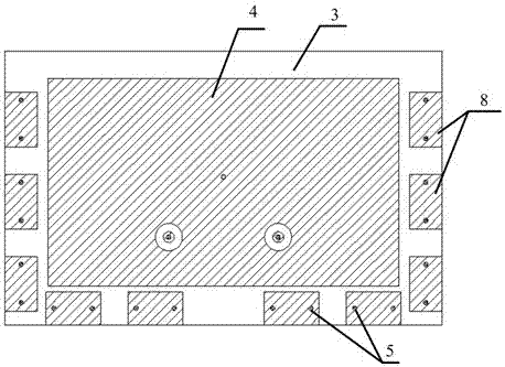
[0013] A three-dimensional differential on-chip antenna based on through-silicon vias, including: a high-resistance silicon substrate 1, a top silicon dioxide layer 2, a bottom silicon dioxide layer 3, and a metal floor 4, and also includes: through-silicon vias 5, differential feeders 6 , a top metal strip 7 , a bottom metal strip 8 and a terminal short-circuit matching line 9 .

[0014] The three-dimensional structural differential on-chip antenna based on through-silicon vias, from bottom to top, is the metal floor 4, the bottom metal strip 8, the bottom silicon dioxide layer 3, the high-resistance silicon substrate 1, the top silicon dioxide layer 2, and the terminal short-circuit matching line 9 , a differential feeder 6 and a top metal strip 7 . The metal floor 4 has a rectangular structure and is placed at the bottom of the entire on-chip antenna. The bottom silicon dioxide layer 3 , the high-resistance silicon substrate 1 and the top silicon dioxide layer 2 are all re...


PUM


Abstract

The invention discloses a three-dimensional differential on-chip antenna based on a silicon through hole, and the antenna comprises a high-resistance silicon substrate (1), a top silicon dioxide layer(2), a bottom silicon dioxide layer (3) and a metal ground plate (4). The antenna also comprises the silicon through hole (5), a differential feed line (6), a top metal strip (7), a bottom metal strip (8), and a terminal short-circuit matching line (9). During operation, a differential radio frequency signal enters the top metal strip (7) connected with the other end of the differential feed line(6) through the silicon through hole (5) at one end of the differential feed line (6). The top metal strip (7) is connected with the bottom metal strip (8) are connected through the silicon through hole (5) to form a double-layer metal strip. A radio frequency signal is transmitted outwards through the double-layer metal strip. The three-dimensional and miniature on-chip antenna based on the silicon through hole (5) is achieved, and the antenna meets the demands of the differential feed when the antenna is connected with a chip, and is suitable for the three-dimensional stacked highly-integrated application of a microsystem antenna and a functional chip.

Description

technical field [0001] The invention relates to an on-chip antenna, in particular to a three-dimensional structure differential on-chip antenna based on through-silicon holes. Background technique [0002] At present, the existing on-chip antenna has a wide range of application requirements in microsystem applications. This type of antenna generally adopts a planar structure. Since the antenna size is related to the wavelength of the antenna's working frequency band, it is difficult for a planar antenna to achieve a small size in a lower frequency band. Moreover, a planar antenna cannot meet the three-dimensional stacking integration of antennas and functional chips. Therefore, it is difficult for the on-chip antenna working in the lower frequency band to be highly integrated with the chip. In addition, traditional on-chip antennas are mostly in the form of single-point feeding. If they are interconnected with chips that use differential signal pins, they need to pass throu...

Claims


Application Information

Patent Timeline
Patent Type & Authority Applications(China)
IPC IPC(8): H01Q1/22H01L23/66
Inventor 王磊刘涓徐国兵
Owner BEIJING INST OF REMOTE SENSING EQUIP
Learn More