Insulator surface charge rapid dissipation method and device based on X-rays
A surface charge and insulator technology, applied in the field of electricity, can solve problems such as high cost, complicated material processing technology, and damage to material integrity, and achieve the effects of ensuring integrity, simple operation, and flexible design
- Summary
- Abstract
- Description
- Claims
- Application Information
AI Technical Summary
Problems solved by technology
Method used
Image
Examples
Embodiment 1
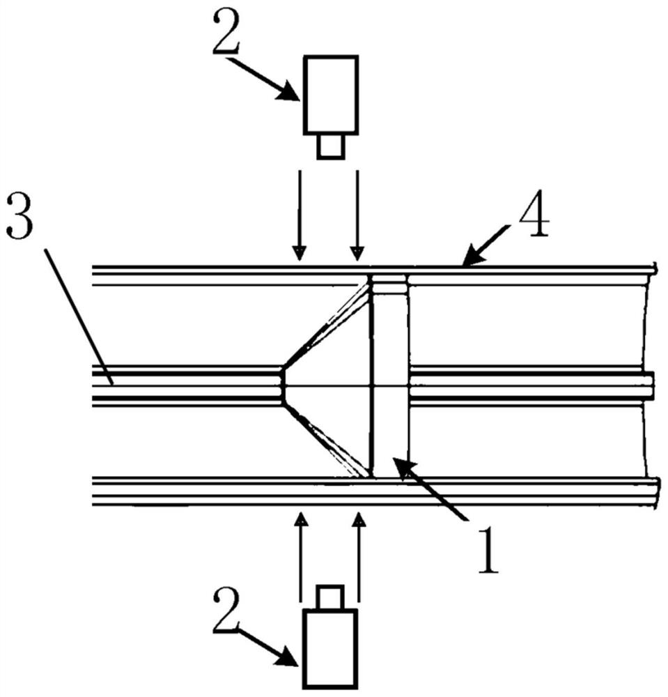
[0033] The principle of the present invention is as follows: X-ray wavelength is about 0.012-0.005 nanometers, and has relatively high energy. Therefore, X-rays are used to irradiate the surface of the insulator that has accumulated charges. The surface charges absorb X-rays and have higher energy to get rid of the traps on the surface of the material, thereby accelerating their dissipation along the surface. In addition, the charged particles generated by the ionization of the surrounding gas neutralize the surface heteropolar charges, effectively reducing the accumulated surface charge. Due to the insulating gas (such as SF 6 , SF 6 with N 2 Mixed gas) has self-recovery properties, and will restore its insulating properties by itself after the irradiation is over.
[0034] In order to reduce the charge accumulated on the surface of the insulator, the X-ray source is pre-installed outside the GIL pipe, such as figure 1 shown. By adjusting the number, angle and position o...
Embodiment example 2
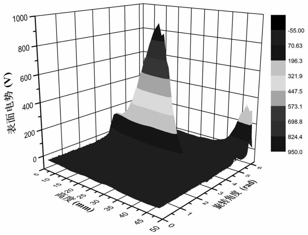
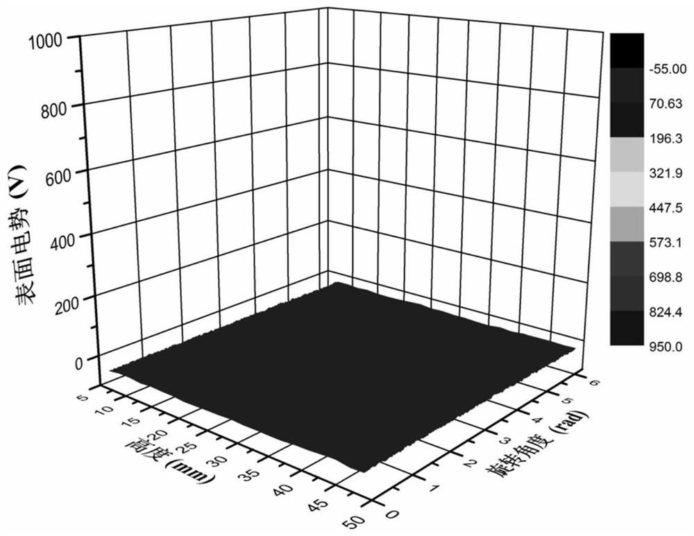
[0038] After 14 minutes of corona discharge, the surface potential distribution of the insulator before and after X-ray irradiation is as follows: Figure 3a and Figure 3b shown.
[0039] The surface potential distribution of the insulator after irradiation is significantly lower than that before irradiation, further verifying the effectiveness of X-ray irradiation for reducing surface charge accumulation.
Embodiment 3
[0041]When the real-time monitoring method is required to accurately dissipate the charge on the surface of the insulator, it is necessary to use a capacitive electrostatic probe to detect the electrostatic voltage of the insulator. However, in order to improve the spatial resolution of the probe measurement, the existing capacitive electrostatic probe often uses Cylindrical design, the introduction of the probe will distort the initial two-dimensional axisymmetric electric field inside the GIL.
[0042] For this reason Figure 4 and 5 As shown, the present invention uses a new electrostatic probe for electrostatic detection. The new electrostatic probe is composed of three symmetrically distributed fan-shaped copper electrodes, and the electrodes are effectively insulated by epoxy resin. The new probe has a ring structure as a whole, which can effectively reduce the influence of the probe installation on the two-dimensional axisymmetric electric field of the GIL. In additio...
PUM
| Property | Measurement | Unit |
|---|---|---|
| length | aaaaa | aaaaa |
| wavelength | aaaaa | aaaaa |
Abstract
Description
Claims
Application Information
 - R&D
- Intellectual Property
- Life Sciences
- Materials
- Tech Scout
- Unparalleled Data Quality
- Higher Quality Content
- 60% Fewer Hallucinations
Browse by: Latest US Patents, China's latest patents, Technical Efficacy Thesaurus, Application Domain, Technology Topic, Popular Technical Reports.
© 2025 PatSnap. All rights reserved.Legal|Privacy policy|Modern Slavery Act Transparency Statement|Sitemap|About US| Contact US: help@patsnap.com


