Efficient ceramic packaging process
A ceramic packaging and process technology, which is applied in the manufacture of electrical components, electrical solid devices, semiconductor/solid devices, etc., can solve problems such as unsatisfactory and rising labor costs, and achieve the goal of improving efficiency, increasing output, and improving process integration. Effect
- Summary
- Abstract
- Description
- Claims
- Application Information
AI Technical Summary
Problems solved by technology
Method used
Image
Examples
Embodiment 1
[0053] An efficient ceramic packaging process includes the following steps:
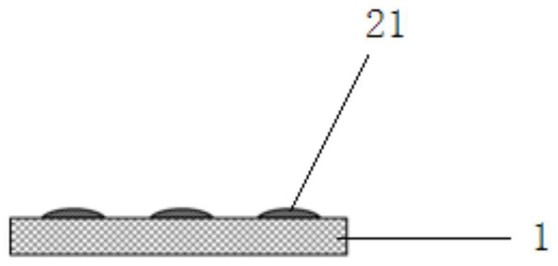
[0054] Step a1, coating the upper surface of the steel tube shell carrier 1 with a thickness of 2 mm and applying a pyrolytic bond temporary bonding adhesive 21 with a fluidity of 100 to 300 pa·s to improve the adhesive strength. wettability and increase the bonding area to the shell carrier 1 and the ceramic shell 3;
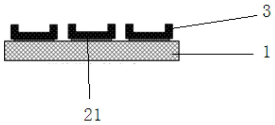
[0055] Step b1, the ceramic shells 3 are placed on the upper surface of the shell carrier 1 in batches and arrayed with the temporary bonding glue 21 through the pyrolysis bond, so that the lateral spacing between adjacent ceramic shells 3 is equal , The longitudinal spacing is equal to form an array of ceramic shells;
[0056] Step c1: Baking the array of ceramic shells, the baking temperature is controlled at 125°C, so that the thermal bond temporary bonding glue 21 is cured, so as to increase the adhesion between the ceramic shell 3 and the shell carrier 1;
[0057] Step d1, taki...
Embodiment 2
[0062] An efficient ceramic packaging process includes the following steps:
[0063]Step a2, coating the upper surface of the glass shell carrier 1 with a light transmittance of 90% and applying a temporary bonding glue 22 for corrosion and debonding;
[0064] Step b2, the ceramic shells 3 are debonded by corrosion and the temporary bonding glue 22 is placed in batches and arrayed and pressed on the upper surface of the shell carrier 1, so that the lateral spacing between adjacent ceramic shells 3 is equal , The longitudinal spacing is equal to form an array of ceramic shells;
[0065] Step c2, irradiating the ceramic package array with UV light from the bottom of the package carrier 1 to cure the temporary bonding glue 22 for corrosion and debonding, so as to increase the bonding between the ceramic package 3 and the package carrier 1 force;
[0066] Step d2, taking the position of the ceramic package 3 as a reference to complete the mounting step of the ceramic sealing cap...
Embodiment 3
[0071] An efficient ceramic packaging process includes the following steps:
[0072] Step a3, coating the upper surface of the glass shell carrier 1 with a light transmittance of 90% and applying a temporary bonding glue 23 for laser debonding;
[0073] Step b3, the ceramic shells 3 are debonded by laser and the temporary bonding glue 23 is batched and arrayed and mounted and pressed on the upper surface of the shell carrier 1, so that the lateral distance between adjacent ceramic shells 3 is equal , The longitudinal spacing is equal to form an array of ceramic shells;
[0074] Step c3, baking the array of ceramic shells, so that the laser debonding temporary bonding glue 23 is cured, so as to increase the adhesive force between the ceramic shell 3 and the shell carrier 1;
[0075] Step d3, taking the position of the ceramic package 3 as a reference to complete the mounting step of the ceramic sealing cap 4 on the ceramic package 3 to form a ceramic package;
[0076] Step e3...
PUM
| Property | Measurement | Unit |
|---|---|---|
| thickness | aaaaa | aaaaa |
| wavelength | aaaaa | aaaaa |
| hardness | aaaaa | aaaaa |
Abstract
Description
Claims
Application Information
 - R&D
- Intellectual Property
- Life Sciences
- Materials
- Tech Scout
- Unparalleled Data Quality
- Higher Quality Content
- 60% Fewer Hallucinations
Browse by: Latest US Patents, China's latest patents, Technical Efficacy Thesaurus, Application Domain, Technology Topic, Popular Technical Reports.
© 2025 PatSnap. All rights reserved.Legal|Privacy policy|Modern Slavery Act Transparency Statement|Sitemap|About US| Contact US: help@patsnap.com


