Quantum dot light-emitting diode, preparation method of quantum dot light-emitting diode
A quantum dot light-emitting and diode technology, applied in semiconductor/solid-state device manufacturing, nanotechnology for materials and surface science, organic semiconductor devices, etc., can solve problems such as poor conductivity, reduce the impact of device performance, and improve performance. , the effect of improving electrical conductivity
- Summary
- Abstract
- Description
- Claims
- Application Information
AI Technical Summary
Problems solved by technology
Method used
Image
Examples
preparation example Construction
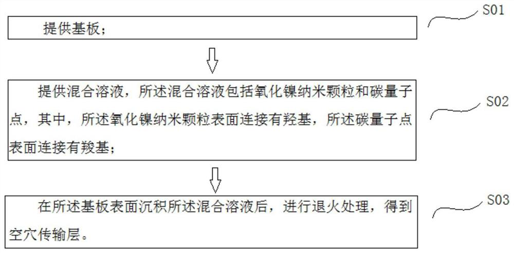
[0031] Correspondingly, such as image 3 As shown, the second aspect of the present invention provides a method for preparing a quantum dot light-emitting diode, comprising the following steps:
[0032] S01. Provide the substrate;
[0033]S02. A mixed solution is provided, the mixed solution includes nickel oxide nanoparticles and carbon quantum dots, wherein the surface of the nickel oxide nanoparticles is connected to a hydroxyl group, and the surface of the carbon quantum dots is connected to a carboxyl group;
[0034] S03. After depositing the mixed solution on the surface of the substrate, perform annealing treatment to obtain a hole transport layer.
[0035] In the method for preparing a quantum dot light-emitting diode provided in the embodiment of the present invention, a mixed solution of nickel oxide nanoparticles and carbon quantum dots is deposited on the surface of a substrate and then annealed to prepare a hole transport layer. The material of the obtained hole...
Embodiment 1
[0067] A preparation method of nickel oxide nanomaterials, comprising the following steps:
[0068] Add an appropriate amount of nickel chloride to 50ml of methanol to form a nickel chloride solution with a total concentration of 1mol / L, stir and dissolve at 60°C, add sodium hydroxide dropwise to dissolve in lye of 10ml of methanol (OH - : Ni 2+ The molar ratio is 2:1 ratio), continue stirring at 60°C for 3h to obtain a homogeneous transparent solution.
[0069] Dissolve an appropriate amount of benzoic acid in 50ml ODE to form a benzoic acid solution with a concentration of 1mol / L; transfer the benzoic acid solution to a polytetrafluoroethylene liner, and place it in a reactor. In a preheated oven, react at a reaction temperature of 250° C. for 3 hours. After the reaction, precipitate and wash with acetone, and centrifuge to prepare carbon quantum dots.
[0070] Disperse an appropriate amount of carbon quantum dots in 50ml of mixed acid (volume ratio of concentrated sulfur...
Embodiment 2
[0074] A preparation method of nickel oxide nanomaterials, comprising the following steps:
[0075] Add an appropriate amount of nickel nitrate to 50ml propanol to form a nickel nitrate solution with a total concentration of 1mol / L, stir and dissolve at 80°C, add ethanolamine dropwise to dissolve in 10ml propanol lye (OH - : Ni 2+ The molar ratio is 2:1); continue to stir at 80° C. for 3 h to obtain a homogeneous transparent solution.
[0076] Dissolve an appropriate amount of phthalic acid in 50ml 1-hexadecene to form a phthalic acid solution with a concentration of 1mol / L; transfer the phthalic acid solution to a polytetrafluoroethylene liner and place it in a reaction kettle , after tightening and sealing the reactor, put it into a preheated oven, and react for 3 hours at a reaction temperature of 250°C. After the reaction, precipitate and wash with acetone, and centrifuge to prepare carbon quantum dots.
[0077] Disperse an appropriate amount of carbon quantum dots in 5...
PUM
| Property | Measurement | Unit |
|---|---|---|
| thickness | aaaaa | aaaaa |
Abstract
Description
Claims
Application Information
 - R&D
- Intellectual Property
- Life Sciences
- Materials
- Tech Scout
- Unparalleled Data Quality
- Higher Quality Content
- 60% Fewer Hallucinations
Browse by: Latest US Patents, China's latest patents, Technical Efficacy Thesaurus, Application Domain, Technology Topic, Popular Technical Reports.
© 2025 PatSnap. All rights reserved.Legal|Privacy policy|Modern Slavery Act Transparency Statement|Sitemap|About US| Contact US: help@patsnap.com


