
Optical device and packaging method thereof

An optical device, height-oriented technology

Active Publication Date: 2020-09-25
GUANGXUN SCI & TECH WUHAN
View PDF5 Cites 0 Cited by
  • Summary
  • Abstract
  • Description
  • Claims
  • Application Information

AI Technical Summary

Problems solved by technology

[0002] In existing optical communication systems, it is very common for optical devices to be packaged in airtight housings. The signal transmission of optical devices is usually conducted by flexible circuit boards. With the continuous improvement of optical communication systems, the transmission rate is 25Gbps and above. In rate transmission applications, the impact of high-frequency signal loss between the flexible circuit board and the airtight housing is becoming more and more obvious, which leads to the deterioration of the indicators of the transmitting end or receiving end and affects the overall transmission performance of optical devices

Method used


Image

  • Optical device and packaging method thereof
  • Optical device and packaging method thereof
  • Optical device and packaging method thereof

Examples


Embodiment Construction

[0032] It should be noted that, in the case of no conflict, the embodiments in the application and the technical features in the embodiments can be combined with each other. Undue Limitation of This Application. In the description of the embodiments of the present application, the orientations and positional relationships of "top", "bottom", "upper" and "lower" refer to the orientation and positional relationship of optical devices in normal use, for example, the attached figure 1 In the directions and positional relationships shown, "μm" refers to the SI unit of micrometer, and "mm" refers to the SI unit of millimeter. The present application will be further described in detail below in conjunction with the accompanying drawings and specific embodiments.

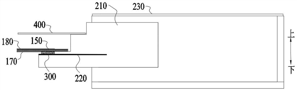
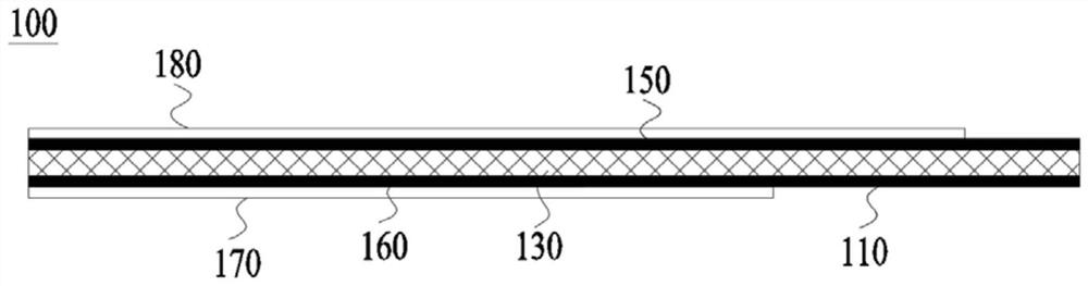
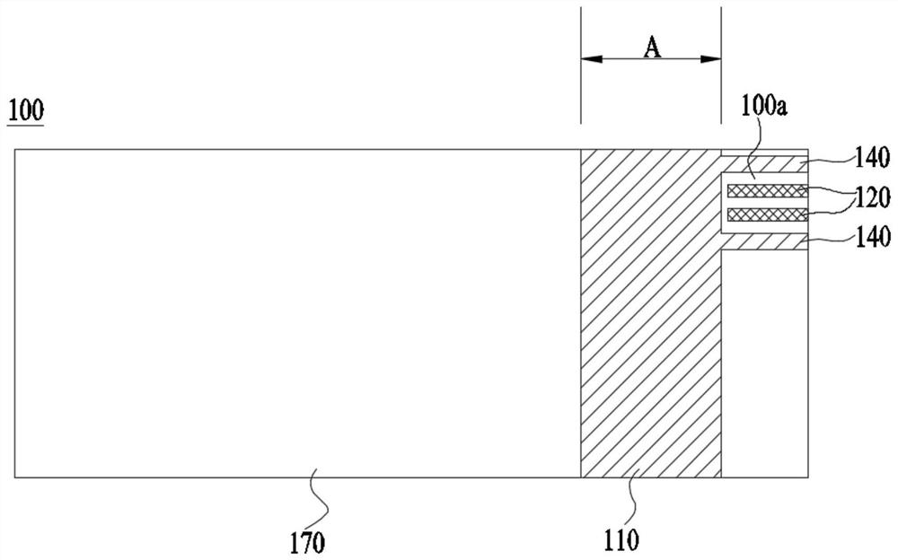
[0033] See Figure 1 to Figure 5 On the one hand, the embodiment of the present application provides an optical device, and the optical device includes a flexible circuit board 100 , a package 200 and a conductive connect...


PUM


Abstract

The invention provides an optical device and a packaging method thereof. The optical device comprises a flexible circuit board, a tube shell and a conductive connecting piece. The flexible circuit board comprises a first reference ground bonding pad, a first signal bonding pad and a dielectric layer. The first reference ground bonding pad and the first signal bonding pad are positioned on the samesurface of the dielectric layer. The tube shell comprises a second reference ground bonding pad, a second signal bonding pad and a substrate. A first step surface and a second step surface adjacent to the first step surface are formed on the surface of one side of the substrate. On the height direction of the substrate, the second step surface is higher than the first step surface. the second signal bonding pad is located on the second step surface, the second reference ground bonding pad is located on the first step surface, the first signal bonding pad is connected with the second signal bonding pad, an accommodating space is formed between the first reference ground bonding pad and the second reference ground bonding pad, and the conductive connecting piece fills the accommodating space to connect the first reference ground bonding pad and the second reference ground bonding pad.

Description

technical field [0001] The present application relates to the technical field of optical communication, and in particular to an optical device and a packaging method thereof. Background technique [0002] In existing optical communication systems, it is very common for optical devices to be packaged in airtight housings. The signal transmission of optical devices is usually conducted by flexible circuit boards. With the continuous improvement of optical communication systems, the transmission rate is 25Gbps and above. In speed transmission applications, the impact of high-frequency signal loss between the flexible circuit board and the airtight housing is becoming more and more obvious, which leads to the deterioration of the indicators of the transmitting end or receiving end and affects the overall transmission performance of the optical device. Contents of the invention [0003] In view of this, the embodiments of the present application hope to provide an optical devic...

Claims


Application Information

Patent Timeline
IPC IPC(8): H05K1/11H05K1/02
CPCH05K1/111H05K1/0237
Inventor 段启金吕妮娜宋旭宇李霄丁深
Owner GUANGXUN SCI & TECH WUHAN
Learn More