A flexible circuit board and corresponding optical module
A technology of flexible circuit boards and optical modules, applied in the field of optical communications, can solve problems affecting wiring impedance matching, high-speed signal mismatch, shortening of solder resistance sections, etc., to reduce manufacturing difficulty and processing costs, and realize high-speed signal matching Transmission, avoiding the effect of impedance mutation
- Summary
- Abstract
- Description
- Claims
- Application Information
AI Technical Summary
Problems solved by technology
Method used
Image
Examples
Embodiment 1
[0034] At present, the high-speed signal transmission network has a trace width difference jump at the connection between the pad and the signal line, and the impedance at the jump is discontinuous. The excited electromagnetic radiation not only weakens the effective signal transmission, but also brings parasitic crosstalk. To solve this problem, This embodiment provides a flexible circuit board.
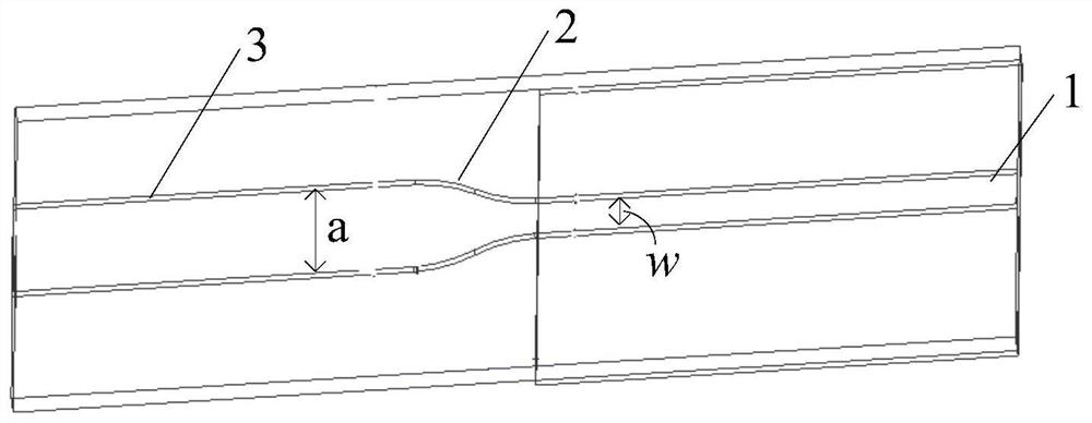
[0035] refer to image 3 , the embodiment of the present invention provides a flexible circuit board, the flexible circuit board includes: a signal transmission line 1, an impedance matching line 2 and a pad 3, and the impedance matching line 2 connects the signal transmission line 1 and the pad 3 .
[0036] Wherein, the width corresponding to the signal transmission line 1 is smaller than the width corresponding to the pad 3, the impedance matching line 2 changes gradually, and the width of the impedance matching line 2 is along the direction close to the pad 3 Gradually increase...
Embodiment 2
[0063] Based on the description of the foregoing embodiments, a set of specific parameters is used for supporting explanations. Here, a single-ended 50-ohm impedance line is used as an example to transmit a 25Gbit / s high-speed signal. The thickness of the substrate is 0.05mm±0.01mm, the dielectric constant of the substrate is 3.2±0.05, and the loss tangent angle is 0.002±0.001. The width of the pad is 0.25mm±0.01mm (that is, a=0.25mm±0.01mm), the distance between the pad and the signal transmission line is 0.2mm±0.01mm (that is, a=0.2mm±0.01mm), and the thickness of the cover film is 0.025mm± 0.01mm, the dielectric constant of the covering film is 3.5±0.05.
[0064] Combining the above parameters, according to the formula three of the embodiment 1, the line width of the signal transmission line is calculated to be 0.1mm (that is, w=0.1mm), and a=0.25mm±0.01mm, w=0.1mm and a=0.2mm± Substitute 0.01mm into formula 1 and formula 2 to obtain the first gradient curve and the second...
PUM
 Abstract
Description
Claims
Application Information
 - Generate Ideas
- Intellectual Property
- Life Sciences
- Materials
- Tech Scout
- Unparalleled Data Quality
- Higher Quality Content
- 60% Fewer Hallucinations
Browse by: Latest US Patents, China's latest patents, Technical Efficacy Thesaurus, Application Domain, Technology Topic, Popular Technical Reports.
© 2025 PatSnap. All rights reserved.Legal|Privacy policy|Modern Slavery Act Transparency Statement|Sitemap|About US| Contact US: help@patsnap.com


