CMOS image sensor capable of improving frame frequency high-speed full-digital data reading
An image sensor and data readout technology, applied in image communication, color TV parts, TV system parts, etc., can solve the problem of increasing the complexity of chip post-processing, reducing the frame rate of super large area array CMOS image sensors, etc. problems, to achieve the effects of reducing delay time, expanding dynamic range, and low noise
- Summary
- Abstract
- Description
- Claims
- Application Information
AI Technical Summary
Problems solved by technology
Method used
Image

Examples
Embodiment 1
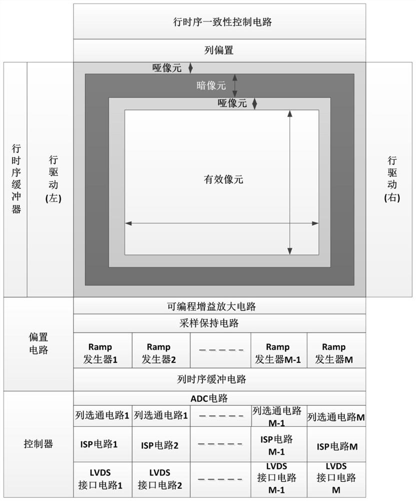
[0044] Such as figure 1 , the photosensitive area array composed of effective pixels, dummy pixels and dark pixels realizes the conversion of photoelectric signals, and the driving ability of the pixel output electrical signal is limited, which is not convenient for transmission, editing and processing. Therefore, the subsequent readout circuit completes the pixel output Electrical signal amplification, noise, storage, analog-to-digital conversion, digital processing, etc. This structure is based on a column-level processing system, and can be divided into a column readout circuit and a column timing buffer circuit according to the location of the module. Peripheral control auxiliary circuits include: timing controllers to realize exposure, conversion, sampling, amplification, readout, AD processing, ISP and other operations; provide bias voltage for column bias, PGA, ADC, Ranp generator, LVDS circuit, etc. Reference module; double-sided drive circuit for large area array row...
Embodiment 2
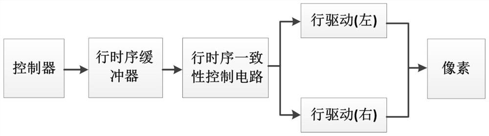
[0046] Such as figure 2 , taking the exposure, conversion and readout sequence control of pixels of a large area array as an example, further illustrating the content of the present invention to improve the frame rate of a large area array.
[0047] The timing of pixel control exposure, conversion and readout output by the controller is firstly buffered by the row timing buffer to realize the row control timing, which reduces the timing delay in the row direction of the large-area array in the path from the controller to the row timing consistency control circuit time; then through the line timing consistency control circuit, the timing consistency of the row driving timing on both sides of the pixel and the timing delay processing in the direction of the large-area array are processed, so that the timing of the row timing reaching the left and right row driving is completely consistent and the delay is the smallest; finally, after the left and right Row drive circuit drive a...
Embodiment 3
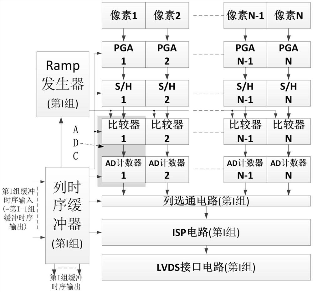
[0049] Such as image 3 , taking the I-th group of readout circuits as a column, the content of the large array column readout circuit of the present invention is further described.
[0050] Group I of the large area array includes N columns of pixels. Firstly, the pixels of this column are sampled and amplified by the programmable gain amplifier (PGA) to realize the sampling and amplification of the pixel reset signal and the integrated signal, and realize the first-level correlated double sampling, and store them in this In the sample-and-hold circuit (S / H) of the column, the voltage difference between the reset signal and the integrated signal represents the light information of the corresponding pixel. The sample-and-hold circuit adopts split-time multiplexing technology, and the programmable gain amplifier can hold the voltage signal on one row while sampling; then, the stored voltage of the sample-and-hold circuit is compared with the slope voltage of the Ramp generator ...
PUM
 Abstract
Description
Claims
Application Information
 - Generate Ideas
- Intellectual Property
- Life Sciences
- Materials
- Tech Scout
- Unparalleled Data Quality
- Higher Quality Content
- 60% Fewer Hallucinations
Browse by: Latest US Patents, China's latest patents, Technical Efficacy Thesaurus, Application Domain, Technology Topic, Popular Technical Reports.
© 2025 PatSnap. All rights reserved.Legal|Privacy policy|Modern Slavery Act Transparency Statement|Sitemap|About US| Contact US: help@patsnap.com