


Quick Research
Generate reliable direction feasibility study reports for your R&D in just a few steps.

Technical Q&A
Discover and master advanced knowledge NOW. Basics, ideas, possibilities, all at once.

Find Solutions
As an expert in R&D theories, this can generate solutions to your technical problems instantly.

Evaluate Feasibility
Analyze your overall solution with one click, know your potential R&D risks in advance.

Monitor Landscape
Get weekly tech updates, stay abreast of the latest tech innovations and key insights.
GaN HEMT semiconductor device and preparation method thereof
A semiconductor and device technology, applied in the field of GaNHEMT semiconductor devices and their preparation, can solve problems such as damage to the performance of metal gate electrodes, and achieve the effects of improving device performance, avoiding damage, and shortening distances
- Summary
- Abstract
- Description
- Claims
- Application Information
AI Technical Summary
Problems solved by technology
Method used
Image

Examples
Embodiment 1
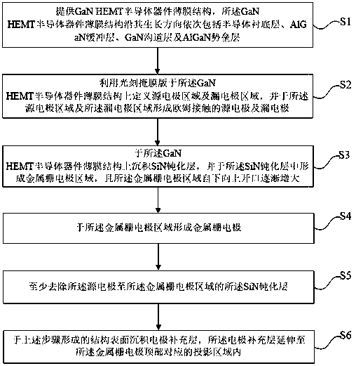
[0049] This embodiment provides a method for manufacturing a GaN HEMT semiconductor device, using a gate-last process (the gate-last process is to prepare the source electrode and the drain electrode first, and then prepare the metal gate electrode) and form a gradually increasing from bottom to top Metal gate electrode, and using the metal gate electrode of this shape as a mask, secondary deposition forms the electrode supplementary layer of the source electrode and the drain electrode, thereby shortening the distance between the source electrode-metal gate electrode and the drain electrode-metal gate electrode, reducing the The access resistance of the source electrode and the drain electrode is reduced, and at the same time, since the metal gate electrode is prepared after the source and drain electrodes, the damage to the metal gate electrode caused by the preparation process of the source and drain electrodes is avoided, and the device performance is improved; In the proce...
Embodiment 2
[0077] Such as Figure 13 to Figure 14 As shown, this embodiment provides another method for preparing a GaN HEMT semiconductor device, which is basically the same as the method for preparing a GaN HEMT semiconductor device in Embodiment 1, except for steps S5 and S6, specifically:
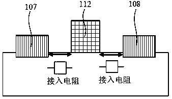
[0078] Such as Figure 13 As shown, in step S5, in this embodiment, the SiN passivation layer 109 in the region from the source electrode 107 to the metal gate electrode 112 is selected to be removed, and the SiN passivation layer 109 in the region from the drain electrode 108 to the metal gate electrode 112 is retained. The SiN passivation layer 109 exposes the source electrode 107, the metal gate electrode 112 and the region between them, and patterned photolithography is used on the remaining part of the SiN passivation layer 109 and on the side of the source electrode 107 Glue 114 for protection. Any suitable method can be used to remove the SiN passivation layer 109, for example, wet BHF or...
Embodiment 3
[0083] This embodiment provides a GaN HEMT semiconductor device. The GaN HEMT semiconductor device can be prepared by the preparation method of the above-mentioned embodiment 1 or embodiment 2, but is not limited to the preparation methods described in embodiment 1 and embodiment 2, as long as it can be formed This GaN HEMT semiconductor device is enough. For the beneficial effects that the GaN HEMT semiconductor device can achieve, please refer to Embodiment 1 and Embodiment 2, and details will not be repeated below.
[0084] Such as Figure 12 and Figure 14 As shown, the GaN HEMT semiconductor device includes:
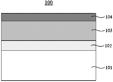
[0085] GaN HEMT semiconductor device thin film structure 100, including a semiconductor substrate layer 101, an AlGaN buffer layer 102, a GaN channel layer 103 and an AlGaN barrier layer 104 stacked in sequence;
[0086] Ohmic contact source electrode 107, drain electrode 108 and metal gate electrode 112 formed on the GaN HEMT semiconductor device thin film structu...
PUM
| Property | Measurement | Unit |
|---|---|---|
| density | aaaaa | aaaaa |
| thickness | aaaaa | aaaaa |
| thickness | aaaaa | aaaaa |
Abstract
Description
Claims
Application Information
 - R&D Engineer
- R&D Manager
- IP Professional
- Industry Leading Data Capabilities
- Powerful AI technology
- Patent DNA Extraction
Browse by: Latest US Patents, China's latest patents, Technical Efficacy Thesaurus, Application Domain, Technology Topic, Popular Technical Reports.
© 2024 PatSnap. All rights reserved.Legal|Privacy policy|Modern Slavery Act Transparency Statement|Sitemap|About US| Contact US: help@patsnap.com