Parallel interleaver, deinterleaver and method suitable for 5G-NR
A 5G-NR and deinterleaver technology, applied in the field of interleaving and deinterleaving, can solve the problems of low efficiency and low throughput, and achieve the effects of simplifying the structure, improving throughput, and increasing parallelism
- Summary
- Abstract
- Description
- Claims
- Application Information
AI Technical Summary
Problems solved by technology
Method used
Image
Examples
Embodiment 1
[0086] A kind of bit interleaver suitable for 5G-NR, its structure is as follows Figure 9 shown.
[0087] Including bit interleaving module A, bit interleaving module B, ping-pong controller, input channel switching module and output channel switching module; wherein, the main tasks of each part are as follows:
[0088]The ping-pong controller is used to monitor the working status of the bit interleaving modules A and B, coordinate and control the cooperation between the bit interleaving modules A and B, and control the switching of the input / output channel modules.
[0089] The bit interleaving module is used to complete the bit interleaving function of the parallel data whose parallel degree is p.
[0090] The input / output channel switching module is used for switching input and output channels according to the instruction of the ping-pong control.
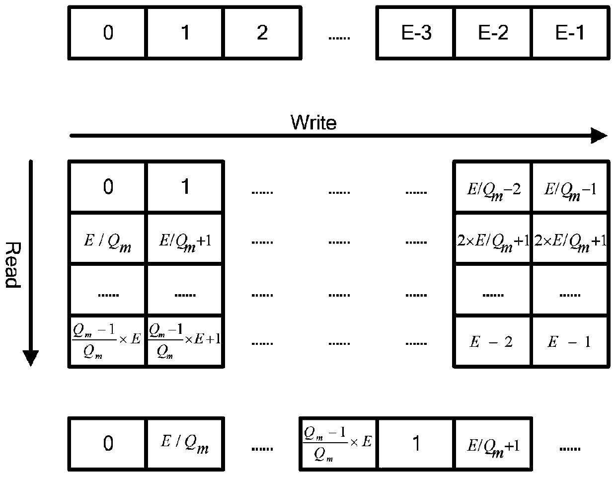
[0091] The interleaved data of each group is obtained according to the interleaving formula. These data are stored row by ...
Embodiment 2
[0095] This embodiment is an example of the specific arrangement of buffers storing data and matrix building blocks when p=32 in embodiment 1, the number of read-write buffers is 8 registers, and the number of RAM memories of matrix building blocks is 9.
[0096] The read-write buffer includes 8 registers REG0~REG7 that can accommodate 32 numbers, and each register stores 32 interleaved data. When Q m =8, the schematic diagram of the parallel data stored in register 0 in the read-write buffer is as follows Figure 12 shown. The read-write buffer interleaves and reads the data read from the virtual matrix and stores them in the register. When the register is full of 8 32-parallel data, the parallel data is sequentially output from registers 0 to 7.
[0097] Different Q m The number of registers to be written is different, and the position of the 32 parallel data written to each register in the read data block is also different. When Q m When they are equal to 2, 4, and 6, r...
Embodiment 3
[0105] Such as Figure 20 As shown, the difference between this embodiment and Embodiment 1 is that the bit interleaving module does not include a read-write buffer, and the output channel switching module is provided with a read-write buffer.
[0106] The functions of the read-write buffers of bit interleaving modules A and B are consistent, and there is no need to consider the problem of data blocking, so further optimization is carried out, and the read-write buffer modules in bit interleaving modules A and B are taken out and placed after the output channel switching module , the two virtual matrices will share this read and write buffer.
[0107] At this time, each memory RAM address is 7bits, and all addresses require a total of 11bits, namely [10:0]. The specific construction method at different values is as follows:
[0108] Q m = 2 hours. Divide RAM8 equally into two parts. The address of each column is 10bit, that is, [9:0], which column is selected by bit[10]...
PUM
 Abstract
Description
Claims
Application Information
 - Generate Ideas
- Intellectual Property
- Life Sciences
- Materials
- Tech Scout
- Unparalleled Data Quality
- Higher Quality Content
- 60% Fewer Hallucinations
Browse by: Latest US Patents, China's latest patents, Technical Efficacy Thesaurus, Application Domain, Technology Topic, Popular Technical Reports.
© 2025 PatSnap. All rights reserved.Legal|Privacy policy|Modern Slavery Act Transparency Statement|Sitemap|About US| Contact US: help@patsnap.com


