Microelectronic packages, flip-chip technology and its application, microelectronic devices

A technology of microelectronic package and process, which is applied in the manufacture of electric solid-state devices, semiconductor devices, semiconductor/solid-state devices, etc., can solve problems affecting the electrical performance of chips, single chip curing, model distortion, etc., to reduce the difficulty of matching, Effect of improving bonding strength and encapsulation efficiency

Active Publication Date: 2022-03-04
FOREHOPE ELECTRONICS NINGBO CO LTD
View PDF5 Cites 0 Cited by
  • Summary
  • Abstract
  • Description
  • Claims
  • Application Information

AI Technical Summary

Problems solved by technology

[0003] The existing flip-chip process has the following disadvantages: First, in the flip-chip process, when there are too many fluxes (such as solder balls) or bumps, it is necessary to use finer-grained glue to fill the bottom first, and then perform plastic sealing. Or the bumps are not easy to touch the bottom conductive block, and they are cured as a single piece, so the efficiency is low
Secondly, the flux needs to be cleaned before underfilling. If the cleaning is not clean, it will cause gaps or holes, and it is easy to fail directly when the board is on the board.
In addition, when filling the bottom, it is necessary to leave no gaps in the filling material, even if the nano-scale layering will cause ion migration, resulting in excessive electrical loss, model distortion, and even functional failure
Furthermore, the reflow soldering temperature generally exceeds 250°C, and the temperature is relatively high, which not only requires higher mechanical properties of the unprotected chip, but also remelts the internal tin bumps when the product is finally placed on the board. If the tin is not fully melted, the tin will be redistributed, and the circuit may be disconnected, seriously affecting the electrical performance of the chip

Method used


Image

  • Microelectronic packages, flip-chip technology and its application, microelectronic devices
  • Microelectronic packages, flip-chip technology and its application, microelectronic devices
  • Microelectronic packages, flip-chip technology and its application, microelectronic devices

Examples


Embodiment Construction

[0042] Embodiments of the present invention will be described in detail below in conjunction with examples, but those skilled in the art will understand that the following examples are only for illustrating the present invention, and should not be considered as limiting the scope of the present invention. Those who do not indicate the specific conditions in the examples are carried out according to the conventional conditions or the conditions suggested by the manufacturer.

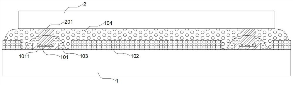
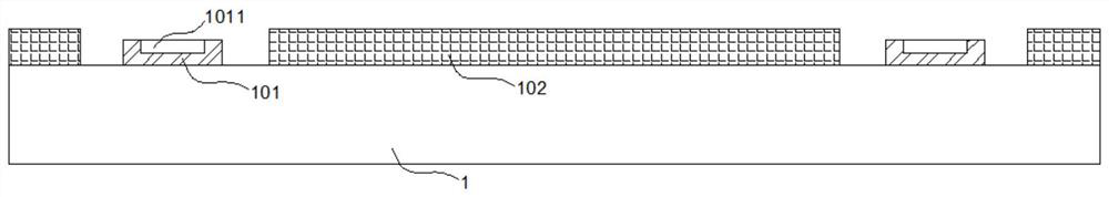
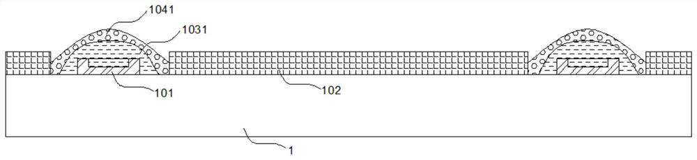
[0043] According to one aspect of the present invention, there is provided a microelectronic package, such as figure 1 As shown, including a substrate 1 and a chip 2, a conductive block 101 is arranged on the substrate 1, a conductive adhesive layer 103 and a non-conductive adhesive layer 104 are arranged on the surface of the conductive block 101 in turn, and a bump 201 is arranged on the chip 2, and the bump 201 presses fit over the conductive block 101.

[0044] The above-mentioned microelectronic pac...


PUM

PropertyMeasurementUnit
lengthaaaaaaaaaa

Abstract

The invention relates to the field of chip packaging, and specifically provides a microelectronic packaging body, a flip-chip process and its application, and a microelectronic device. The flip-chip process of the microelectronic package includes the following steps: (a) providing a substrate provided with a conductive block; (b) sequentially coating conductive glue and non-conductive glue on the surface of the conductive block; The chip is pressed and bonded to the substrate, and then cured to obtain a microelectronic package. The process uses conductive adhesive and non-conductive adhesive, the process is simple, the packaging efficiency is high, the chip function is stable and reliable, the package body is not easy to warp and deform, and the service life is long.

Description

technical field [0001] The invention relates to the field of chip packaging, in particular to a microelectronic packaging body, a flip-chip process and its application, and a microelectronic device. Background technique [0002] The flip-chip packaging process is a packaging technology to improve the packaging speed and component reliability. The traditional solder paste flip-chip assembly process includes: flux coating, chip layout, solder paste reflow and underfill, etc., its primary Design considerations include solder bump and under bump structures, the role of the solder bump is to act as a mechanical, electrical, and sometimes thermal interconnection between the IC and the circuit board. [0003] The existing flip-chip process has the following disadvantages: First, in the flip-chip process, when there are too many fluxes (such as solder balls) or bumps, it is necessary to use finer-grained glue to fill the bottom first, and then perform plastic sealing. Or the bumps ...

Claims


Application Information

Patent Timeline
Patent Type & Authority Patents(China)
IPC IPC(8): H01L23/31H01L21/56H01L23/488H01L21/60
CPCH01L23/31H01L21/56H01L24/11H01L24/13H01L2224/111H01L2224/13016
Inventor 王顺波钟磊庞宏林李利
Owner FOREHOPE ELECTRONICS NINGBO CO LTD
Why Eureka
Try Eureka