A sulfide-silicon nitride suspended waveguide capable of forward Brillouin scattering and its preparation method
A technology of Brillouin scattering and suspended waveguide, which is applied in the direction of optical waveguide, light guide, instrument, etc., can solve the problems of difficult suspended structure, soft vulcanized material, limiting device gain and performance, etc.
- Summary
- Abstract
- Description
- Claims
- Application Information
AI Technical Summary
Problems solved by technology
Method used
Image


Examples
Embodiment 1
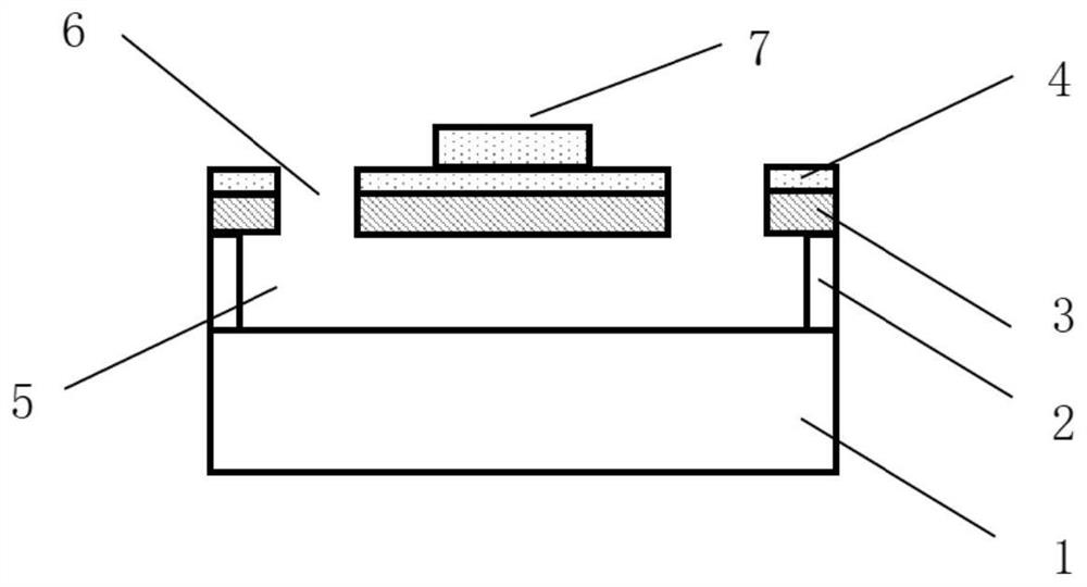
[0027] Such as figure 1 It shows a sulfide-silicon nitride suspended waveguide that can realize forward Brillouin scattering. From bottom to top, there are silicon substrate 1, silicon oxide layer 2, silicon nitride film layer 3, and sulfide film layer 4. ; Both sides of the sulfide thin film layer 4 are etched with a ridge structure 7 of a chalcogenide waveguide; a first air groove 6 is also etched on the sulfide thin film layer 4, and the first air groove 6 is located at the ridge The two sides of the shaped structure 7; the silicon nitride thin film layer 3 and the sulfide thin film layer 4 are etched below the second air groove 5, and the first air groove 6 communicates with the second air groove 5.
[0028] Wherein, the thickness of the silicon substrate 1 is 525 microns or 700 microns. The thickness of the silicon oxide layer 2 is 2 microns-3 microns. The silicon nitride thin film layer 3 is located on the silicon oxide layer 2 and is grown by chemical vapor deposition...
Embodiment 2
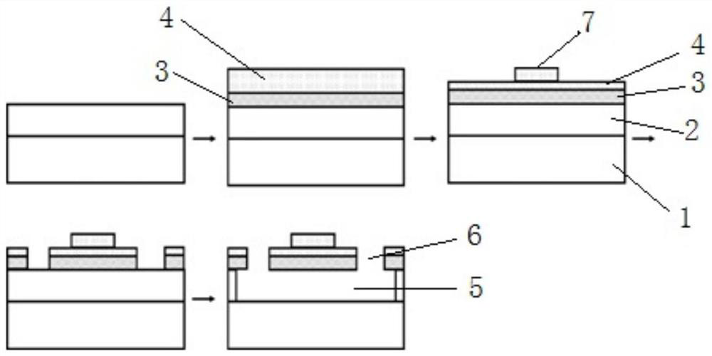
[0030] The present invention also provides a method for preparing a sulfide-silicon nitride suspended waveguide capable of forward Brillouin scattering, such as figure 2 shown, including the following steps:
[0031] S1. On the silicon substrate 1 layer and the silicon oxide layer 2 substrate, a silicon nitride film layer 3 with a thickness of about 100-200 nanometers is grown by chemical vapor deposition;
[0032] S2. Evaporating a 300-500 nanometer sulfide film layer 4 on the silicon nitride film layer 3 by thermal evaporation;
[0033] S3. Etching the ridge structure 7 of the chalcogenide waveguide on the sulfide film layer 4 by using electron beam exposure and dry etching technology, wherein the etching depth of the ridge structure 7 of the chalcogenide waveguide is 200-400 nanometers, The width is 1-2 microns;
[0034] S4. Etching the remaining sulfide and silicon nitride thin film layers 3 on both sides of the ridge waveguide until the silicon oxide layer 2 in the mid...
PUM
| Property | Measurement | Unit |
|---|---|---|
| thickness | aaaaa | aaaaa |
| thickness | aaaaa | aaaaa |
| thickness | aaaaa | aaaaa |
Abstract
Description
Claims
Application Information
 - R&D
- Intellectual Property
- Life Sciences
- Materials
- Tech Scout
- Unparalleled Data Quality
- Higher Quality Content
- 60% Fewer Hallucinations
Browse by: Latest US Patents, China's latest patents, Technical Efficacy Thesaurus, Application Domain, Technology Topic, Popular Technical Reports.
© 2025 PatSnap. All rights reserved.Legal|Privacy policy|Modern Slavery Act Transparency Statement|Sitemap|About US| Contact US: help@patsnap.com