Radio-voltaic nuclear battery based on perovskite crystals
A perovskite and nuclear battery technology, applied in the field of nuclear batteries, can solve problems such as low conversion efficiency, and achieve the effects of large open circuit voltage, large junction thickness, high energy conversion efficiency and output power
- Summary
- Abstract
- Description
- Claims
- Application Information
AI Technical Summary
Problems solved by technology
Method used
Image
Examples
Embodiment 1
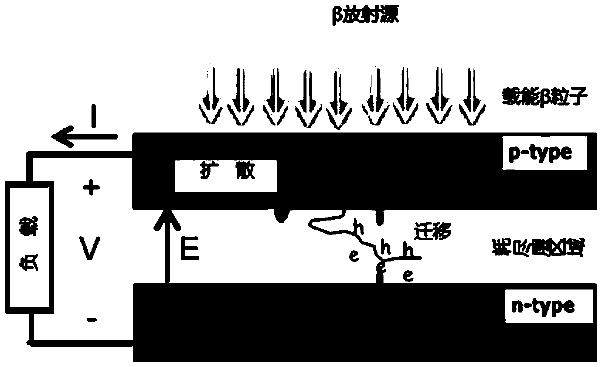
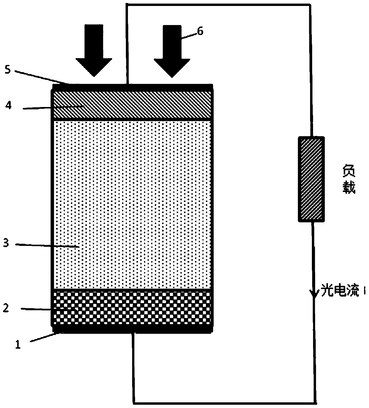
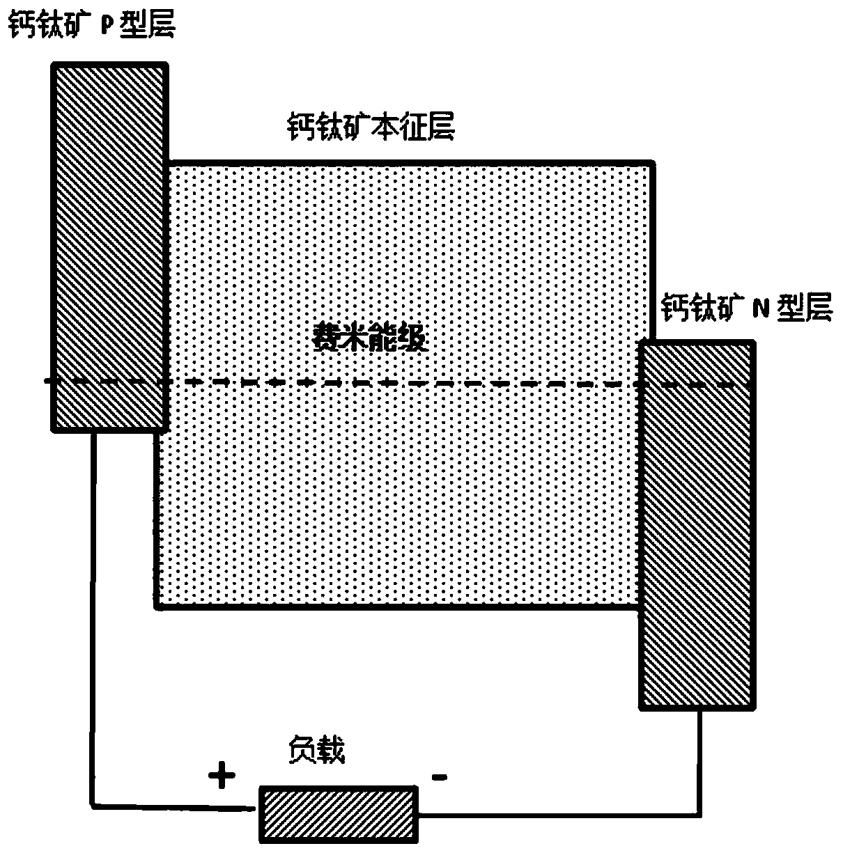
[0025] Embodiment 1: see Figure 1-Figure 4, a radiovoltaic nuclear battery based on perovskite crystals, the structure of the nuclear battery is as follows from top to bottom: radiation source, anode electrode 5, p-type perovskite layer 4, intrinsic perovskite layer 3, n Type perovskite layer 2 and cathode 1. The high-energy particle rays 6 generated by the radiation source are incident on the battery conversion unit from top to bottom. 5 is an anode electrode, and its work function is close to the top of the valence band of the P-type perovskite layer, so as to facilitate the transmission of photogenerated holes. 4 is a P-type perovskite layer, which is mainly used to form a depletion layer to generate photovoltage, and the thickness of the P-type layer is between 0.1mm and 1mm. 3 is the intrinsic perovskite layer, which is mainly used for the absorption and photoelectric conversion of high-energy particles, so its thickness is relatively large. Especially for high-energy...
Embodiment 2
[0026] Example 2: see Figure 1-Figure 4 , a radiation voltaic nuclear battery based on perovskite crystals, the method of epitaxially growing perovskite PIN junction is as follows: step 1) first grow N-type perovskite substrate by variable temperature method, such as Figure 4 (a) shown. Step 2) epitaxially grow thicker intrinsic perovskite crystals on N-type perovskite substrates, such as Figure 4 (b) shown. Step 3) Epitaxial growth of P-type perovskite crystals on intrinsic perovskite crystals, such as Figure 4 As shown in (c), and set a horizontal cutting line and two vertical cutting lines; step 4) split the crystal along the horizontal cutting line and the vertical cutting line to obtain the perovskite PIN junction, as Figure 4 (d) shown. A cathode electrode is deposited on the N-type perovskite layer, and an anode electrode is deposited on the P-type perovskite layer. The perovskite PIN structure was epitaxially grown by solution method. By adjusting the growth...
PUM
 Abstract
Description
Claims
Application Information
 - Generate Ideas
- Intellectual Property
- Life Sciences
- Materials
- Tech Scout
- Unparalleled Data Quality
- Higher Quality Content
- 60% Fewer Hallucinations
Browse by: Latest US Patents, China's latest patents, Technical Efficacy Thesaurus, Application Domain, Technology Topic, Popular Technical Reports.
© 2025 PatSnap. All rights reserved.Legal|Privacy policy|Modern Slavery Act Transparency Statement|Sitemap|About US| Contact US: help@patsnap.com


