Fin type lateral double-diffusion power device

A lateral double-diffusion, power device technology, used in semiconductor devices, semiconductor/solid-state device manufacturing, electrical components, etc., can solve the problems of no modulation in the drift region, no improvement in the drift region, etc., to suppress the short-channel effect. , Good channel control ability, the effect of improving gate leakage current

Active Publication Date: 2020-06-05
NANJING UNIV OF POSTS & TELECOMM +1
View PDF5 Cites 3 Cited by
  • Summary
  • Abstract
  • Description
  • Claims
  • Application Information

AI Technical Summary

Problems solved by technology

In the fin-type process, the LDMOS semiconductor device becomes a fin-type three-dimensional structure, such as the literature: Amin Pak, Ali A.Orouji. Compact Modeling of Fin-LDMOSTransistor Based on the Surface Potential, Silicon, 2019, pp.1-6 involves A fin-type LDMOS device, but this device only uses a three-gate structure for channel modulation, and does not improve the drift region
SMIC International Integrated Circuit Manufacturing (Shanghai) Co., Ltd. proposed a lateral double-diffusion semiconductor device (CN104576732B) of a parasitic FinFET. no modulation

Method used


Image

  • Fin type lateral double-diffusion power device
  • Fin type lateral double-diffusion power device
  • Fin type lateral double-diffusion power device

Examples


Embodiment Construction

[0026] The present invention will be further described in detail below in conjunction with the examples.

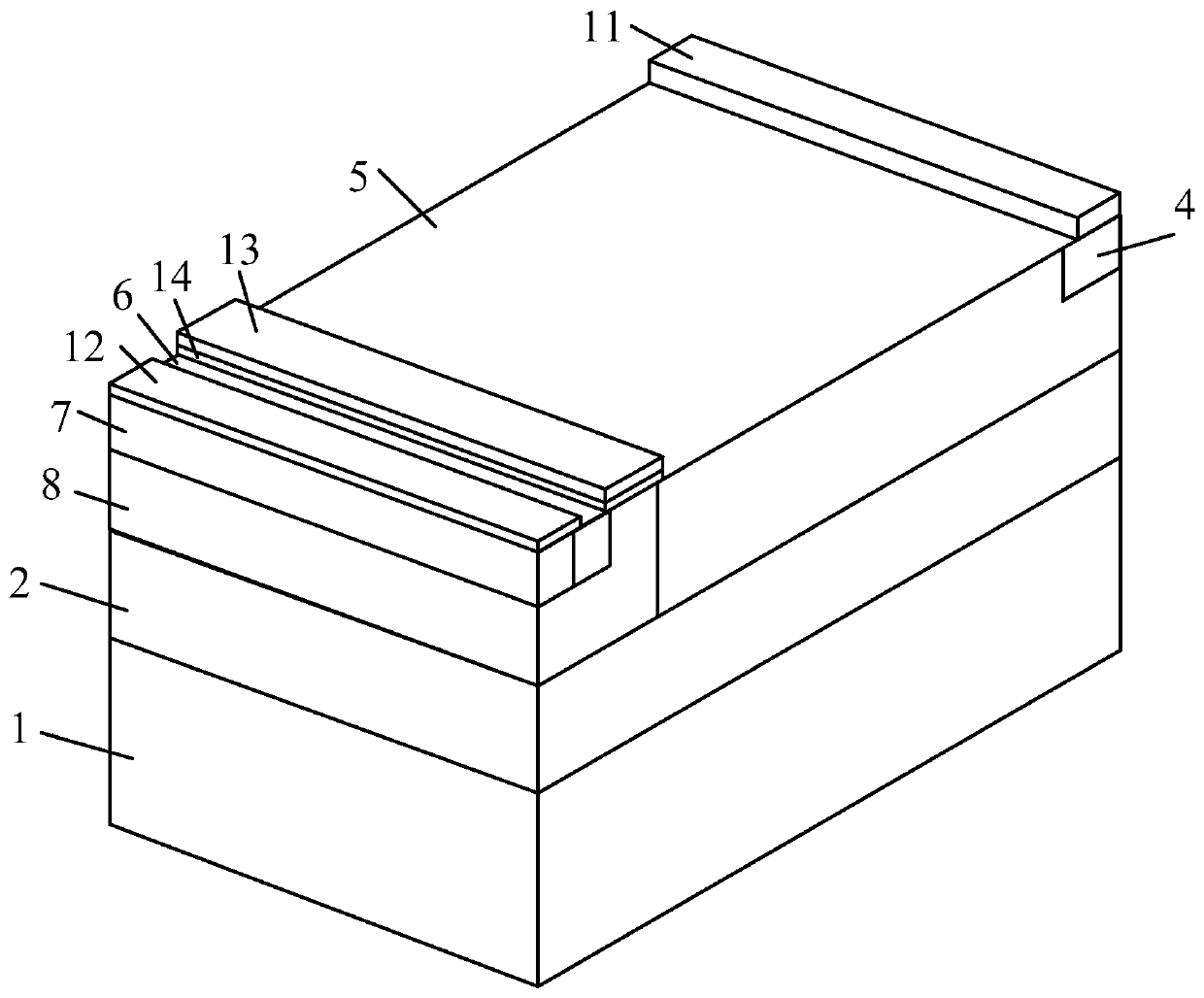
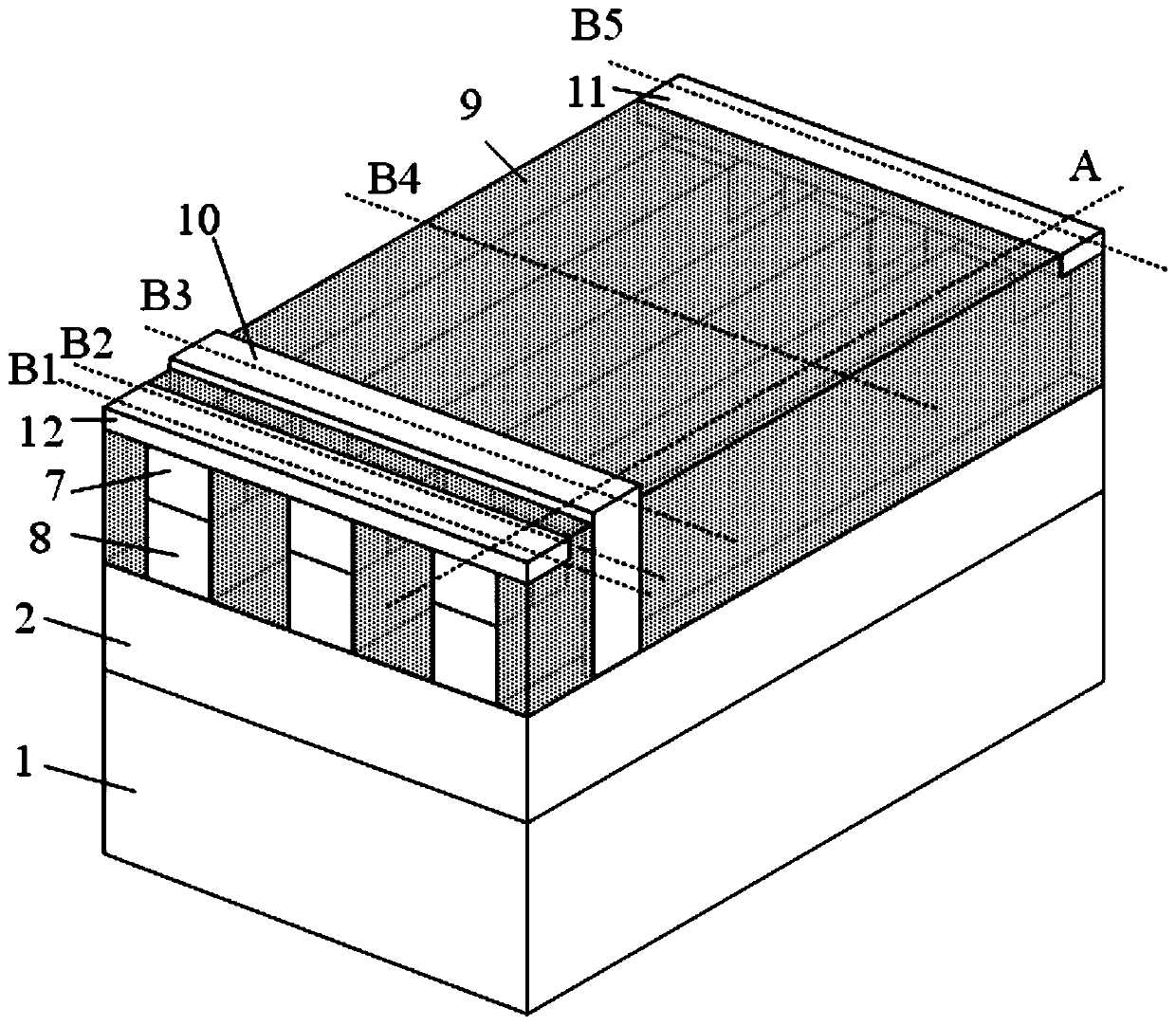
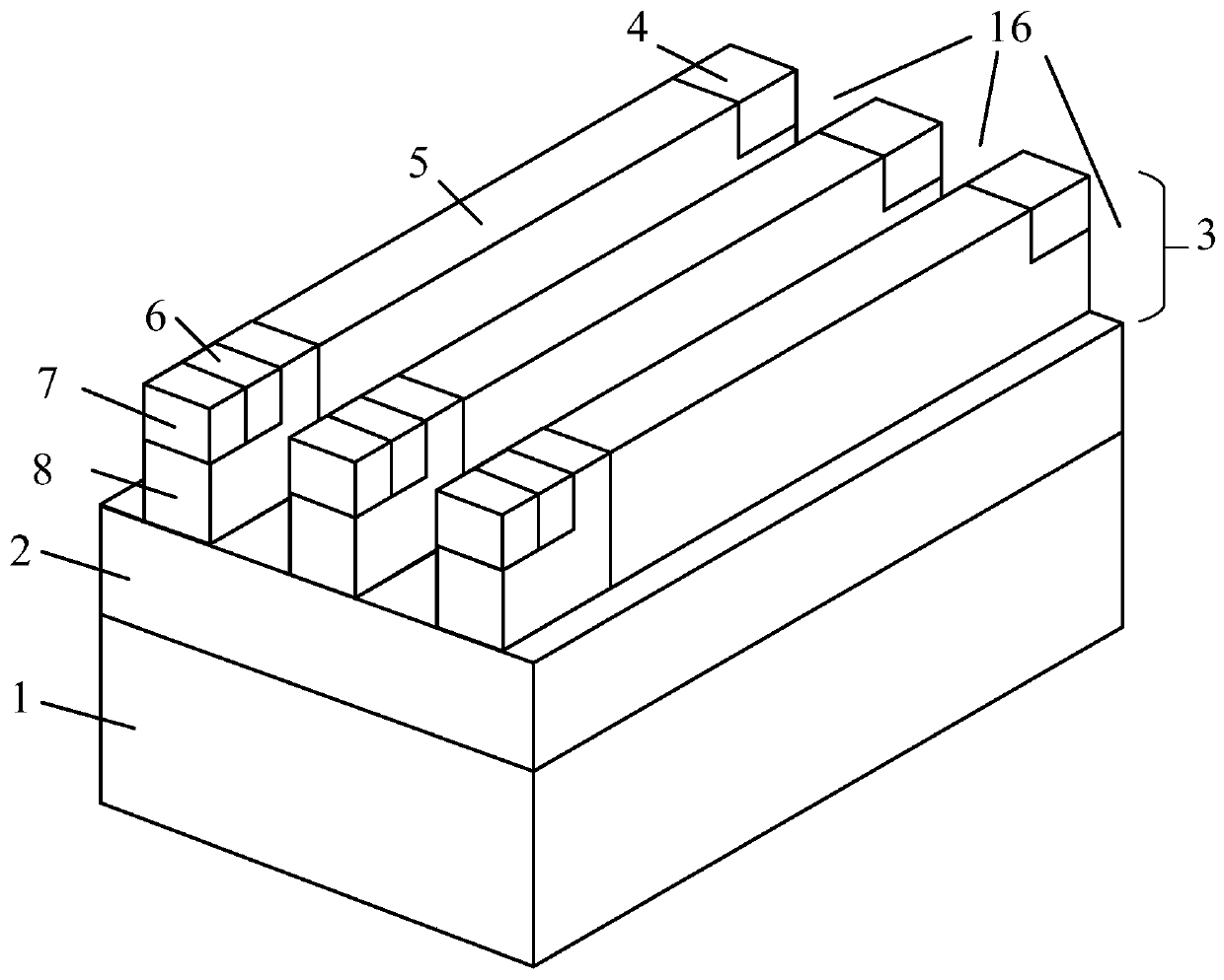
[0027] Such as figure 2 Shown is a fin-type lateral double-diffused power device provided by the present invention, the LDMOS device includes a semiconductor substrate 1 at the bottom, a buried layer 2 on the substrate, and a fin-type active region 3 above the buried layer;

[0028] Such as image 3 As shown, the fin-type active region 3 includes several discrete fins, which are convex, image 3 Three fins are shown in the figure, and dielectric trench regions are arranged on both sides of the fins; each fin includes a semiconductor drain region 4, a semiconductor drift region 5, and a semiconductor well region 8, and the semiconductor well region 8 is located at the edge of the semiconductor drift region 5. On one side, the semiconductor drain region 4 is located above the other side of the semiconductor drift region 5; wherein the semiconductor well region 8 includes...


PUM

PropertyMeasurementUnit
widthaaaaaaaaaa

Abstract

The invention discloses a fin-type lateral double-diffusion power device, which is characterized in that an active region above a substrate is prepared into a fin-type structure, then high dielectricconstant media are adopted to cover the two sides and the surface of a fin-type active region, and modulation is carried out on the active region from three directions; the original surface gate is replaced by the three gates, so that the channel control capability is better, and the leakage current when the device is turned off is reduced; a common silicon oxide gate medium is changed into a high-k gate medium, a thicker physical oxide layer can be achieved, and the problem of gate leakage current is solved. The invention has the advantages of high voltage resistance, low on-resistance, low leakage current and the like, and is suitable for the field of high voltage and high frequency.

Description

technical field [0001] The invention relates to the technical field of semiconductor power devices, in particular to a fin-type lateral double-diffusion power device. Background technique [0002] With the development of power chip design technology, power integrated circuits have put forward higher requirements on the performance of semiconductor power devices. As one of the core devices of power integrated circuits, lateral semiconductor power devices need to provide high breakdown voltage, low On-resistance to reduce power consumption may also require better subthreshold characteristics and avoid short-channel effects. Lateral double-diffusion power device LDMOS is widely used in DC-DC converters and radio frequency base stations due to its good process compatibility, excellent conversion performance, high power performance, high gain and linearity, and low manufacturing cost. . [0003] When the LDMOS breakdown voltage increases, the on-resistance often increases at th...

Claims


Application Information

Patent Timeline
Patent Type & Authority Applications(China)
IPC IPC(8): H01L29/78H01L29/51H01L21/336
CPCH01L29/51H01L29/7816H01L29/7855H01L29/66681H01L29/66803
Inventor 姚佳飞张振宇郭宇锋
Owner NANJING UNIV OF POSTS & TELECOMM
Why Eureka
Try Eureka