Method for preparing hollowed structure on surface of transparent material and in transparent material
A technology of transparent material and hollow structure, applied in the field of femtosecond laser micro-nano processing, can solve the problems of high environmental requirements and low processing efficiency, and achieve the effect of wide application prospects
- Summary
- Abstract
- Description
- Claims
- Application Information
AI Technical Summary
Problems solved by technology
Method used
Image
Examples
Embodiment 1
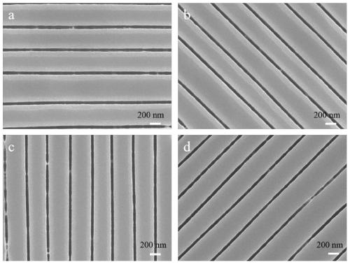
[0030] Quartz surface processing high-precision nanowire array structure
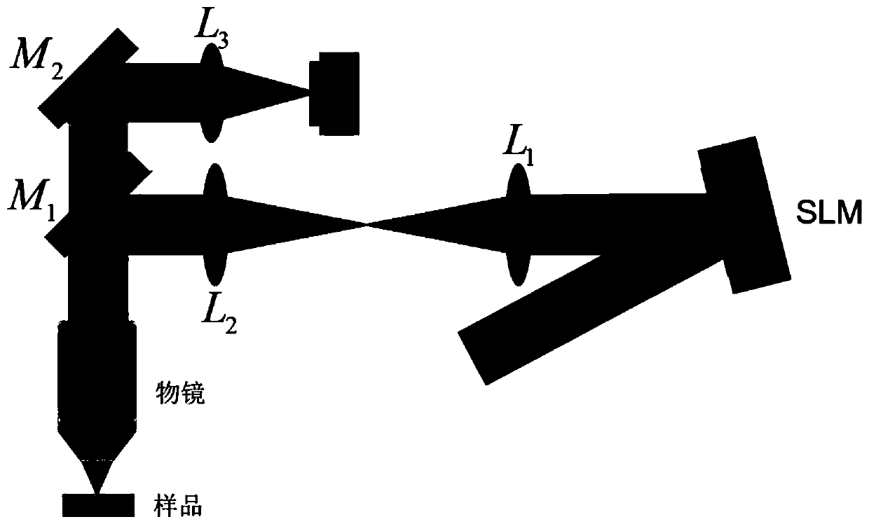
[0031] A femtosecond laser is used to write a uniform line structure inside the quartz, and then the sample is polished to the vicinity of the processing area by mechanical polishing, and then an anisotropic etching is performed by a wet etching process, so as to realize a uniform nanowire array structure on the quartz surface.
[0032] A method for preparing an ultra-high-precision structure on the surface of a transparent hard and brittle material, the specific steps are as follows:
[0033] (1), sample preparation and leveling;
[0034] First, a bulk fused silica sample with a thickness of 500 μm was cut into 20x20mm by a glass knife 2 , placed in acetone and alcohol test tubes for ultrasonic treatment for 20 minutes, and finally placed in a beaker filled with deionized water for 10 minutes, and dried with nitrogen. Then use double-sided adhesive tape to attach the quartz sample to a glass slide, a...
Embodiment 2
[0043] Nanowire Array Structure in 45-degree Direction on YAG Crystal Surface
[0044] A femtosecond laser is used to write a uniform nanometer-precision modified structure inside the YAG crystal, and an ion beam thinner is used to quantitatively thin the surface of the YAG crystal. Finally, an anisotropic etching of the YAG is performed using a wet etching process.
[0045] (1) Leveling of the sample stage:
[0046] Same as example 1.
[0047] (2) Writing of uniform nanostructures inside YAG
[0048] Same as Example 1, the only difference is that different spherical aberration correction holograms are loaded on the spatial light modulator and the single pulse energy used. The single pulse energy used here is 247nJ, and the internal depth is 30um.
[0049] (3) Focused ion beam thinning
[0050] Paste the prepared YAG sample evenly on the aluminum column of the ion beam thinning instrument with quick-drying adhesive, put the aluminum column into the ion beam thinning instru...
PUM
| Property | Measurement | Unit |
|---|---|---|
| thickness | aaaaa | aaaaa |
| thickness | aaaaa | aaaaa |
Abstract
Description
Claims
Application Information
 - R&D
- Intellectual Property
- Life Sciences
- Materials
- Tech Scout
- Unparalleled Data Quality
- Higher Quality Content
- 60% Fewer Hallucinations
Browse by: Latest US Patents, China's latest patents, Technical Efficacy Thesaurus, Application Domain, Technology Topic, Popular Technical Reports.
© 2025 PatSnap. All rights reserved.Legal|Privacy policy|Modern Slavery Act Transparency Statement|Sitemap|About US| Contact US: help@patsnap.com


