Heat dissipation device based on semiconductor wafer and photovoltaic panel power station

A heat dissipation device and semiconductor technology, applied in photovoltaic power generation, semiconductor devices, semiconductor/solid-state device components, etc., can solve problems such as poor heat dissipation performance and lack of temperature difference power generation

Pending Publication Date: 2020-05-08
HUNAN CHUANGHUA LOW CARBON ENVIRONMENTAL PROTECTION TECH
View PDF0 Cites 0 Cited by
  • Summary
  • Abstract
  • Description
  • Claims
  • Application Information

AI Technical Summary

Problems solved by technology

[0019] The technical problem solved by the present invention is to provide a heat sink based on a semiconductor chip to solve the technical problems of poor heat dissipation performance of the chip heat sink in the prior art or lack of technical design for thermoelectric power generation

Method used


Image

  • Heat dissipation device based on semiconductor wafer and photovoltaic panel power station
  • Heat dissipation device based on semiconductor wafer and photovoltaic panel power station
  • Heat dissipation device based on semiconductor wafer and photovoltaic panel power station

Examples


no. 1 example

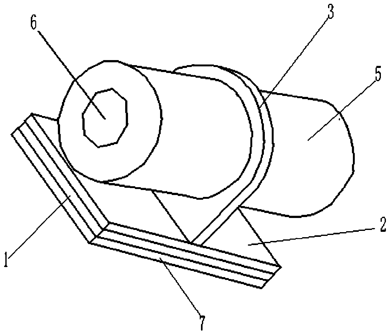
[0074] see figure 1 The heat dissipation device based on the semiconductor wafer provided by the present invention includes a semiconductor wafer 1 and at least one heat conduction component; The heat conduction plate 2, the heat conduction element 5 runs through the heat conduction rib 3, and a fluid channel 6 is formed on the heat conduction element 5;

[0075] The first end surface of the semiconductor chip 1 is attached to the heat conducting plate 2, and the second end surface of the semiconductor chip 1 is attached to the external heat sink 7; the cold fluid passes through the fluid channel 6;

[0076] Wherein, the electric arm on the first end surface of the semiconductor wafer 1 and the electric arm on the second end surface are connected to a DC power supply device, so as to realize heat transfer between the first end surface and the second end surface of the semiconductor wafer 1;

[0077] Alternatively, the electrical arm on the first end surface of the semiconduct...

no. 2 example

[0099] see figure 2 , based on the semiconductor wafer-based heat dissipation device proposed in the first implementation of the present invention, the second embodiment of the present invention proposes another heat dissipation device, the difference is that the number of the conduction and heat transfer elements 4 is Multiple, the conduction and heat transfer elements 4 are guide tubes.

no. 3 example

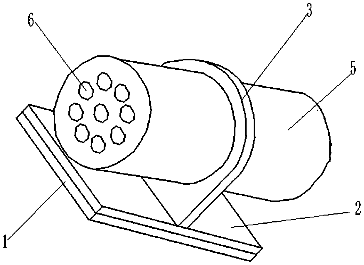
[0101] see image 3 , based on a heat dissipation device based on a semiconductor wafer proposed in the first implementation of the present invention, the third embodiment of the present invention proposes another heat dissipation device, the difference is that the number of the conduction and heat transfer elements 5 is One, the conduction and heat transfer element 5 is a guide post; the guide post is a porous guide post.


PUM


Abstract

The invention provides a heat dissipation device based on a semiconductor wafer. The heat dissipation device comprises the semiconductor wafer and at least one heat conduction assembly. A fluid channel is formed in the flow guide heat transfer piece; the heat dissipation device can realize heat transfer between the first end surface and the second end surface of the semiconductor wafer; or the heat dissipation device can realize thermoelectric power generation between the first end surface and the second end surface of the semiconductor wafer. The heat dissipation device provided by the invention can quickly absorb the heat of the chip and the photovoltaic panel, and timely takes away the heat generated by the operation of the chip; the heat is provided for the semiconductor thermoelectricpower generation chip as a heat source; the semiconductor thermoelectric power generation purpose is achieved through the heat, and the effect of achieving two purposes at a time can be achieved. Theheat dissipation device can be widely applied to many fields such as big data centers, telecommunication machine rooms and photovoltaic power plants, can achieve thermoelectric power generation whileheat dissipation is conducted on photovoltaic panels, LED lamps and chips, and guarantees the efficient, stable and reliable operation of the photovoltaic panels, the LED lamps and the chips.

Description

technical field [0001] The invention relates to the technical field of thermal heat dissipation, in particular to a semiconductor wafer-based heat dissipation device and a photovoltaic panel power station. Background technique [0002] The power consumption of China's data centers exceeds the combined power generation of the Three Gorges and Gezhou Dam. Its staggering power consumption has led many researchers to study various chip cooling technologies, and liquid cooling may become the key to breaking the situation. According to the statistical data center, more than half of the energy consumption is used for cooling equipment, and cooling energy consumption has become the key to the bottleneck of the development of ranks. Although air cooling is still the most commonly used technology in the industry, more and more servers have begun to choose the "bath" cooling method to obtain lower energy consumption cooling methods, but "bath" cooling will also have a negative impact o...

Claims


Application Information

Patent Timeline
IPC IPC(8): H01L23/367H01L23/38H01L23/473H01L31/052H01L31/0525H02S40/42
CPCH01L23/367H01L23/3672H01L23/38H01L23/473H01L31/0521H01L31/0525H02S40/425Y02E10/50
Inventor 刘小江
Owner HUNAN CHUANGHUA LOW CARBON ENVIRONMENTAL PROTECTION TECH
Why Eureka
Try Eureka