


Quick Research
Generate reliable direction feasibility study reports for your R&D in just a few steps.

Technical Q&A
Discover and master advanced knowledge NOW. Basics, ideas, possibilities, all at once.

Find Solutions
As an expert in R&D theories, this can generate solutions to your technical problems instantly.

Evaluate Feasibility
Analyze your overall solution with one click, know your potential R&D risks in advance.

Monitor Landscape
Get weekly tech updates, stay abreast of the latest tech innovations and key insights.
Heat transfer device based on semiconductor wafer and equipment adopting device
A technology of semiconductors and wafers, applied in the field of thermoelectric conversion devices, can solve the problems of inability to efficiently cool and heat semiconductors, lack of thermoelectric power generation, etc., and achieve the effects of high-efficiency heat transfer, high-efficiency cooling and heating
- Summary
- Abstract
- Description
- Claims
- Application Information
AI Technical Summary
Problems solved by technology
Method used
Image

Examples
no. 1 example
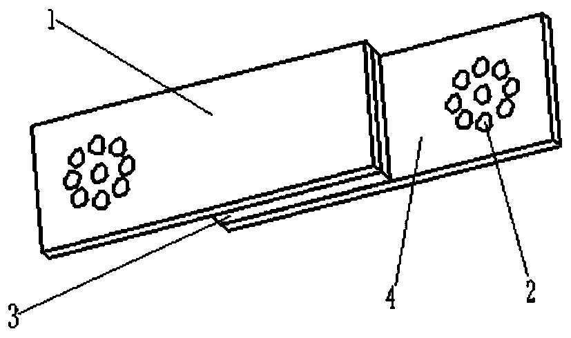
[0098] see figure 1 , the semiconductor wafer-based heat transfer device provided by the present invention includes a semiconductor wafer 3 and two heat conducting plates 1, and the semiconductor wafer 3 is sandwiched between the two heat conducting plates 1;
[0099] Fluid channels 2 are opened on the two heat conducting plates 1;
[0100] The semiconductor wafer 3 is located between the two fluid channels 2; the two fluid channels 2 respectively pass through two fluids with a temperature difference and opposite flow directions;
[0101] Wherein, the electric arm at the first end of the semiconductor wafer 3 and the electric arm at the second end are connected to a DC power supply device, so as to realize heat transfer between the first end surface and the second end surface of the semiconductor wafer 3;
[0102] Alternatively, the electrical arm at the first end and the electrical arm at the second end of the semiconductor wafer 3 are respectively connected to electrical lo...
no. 2 example
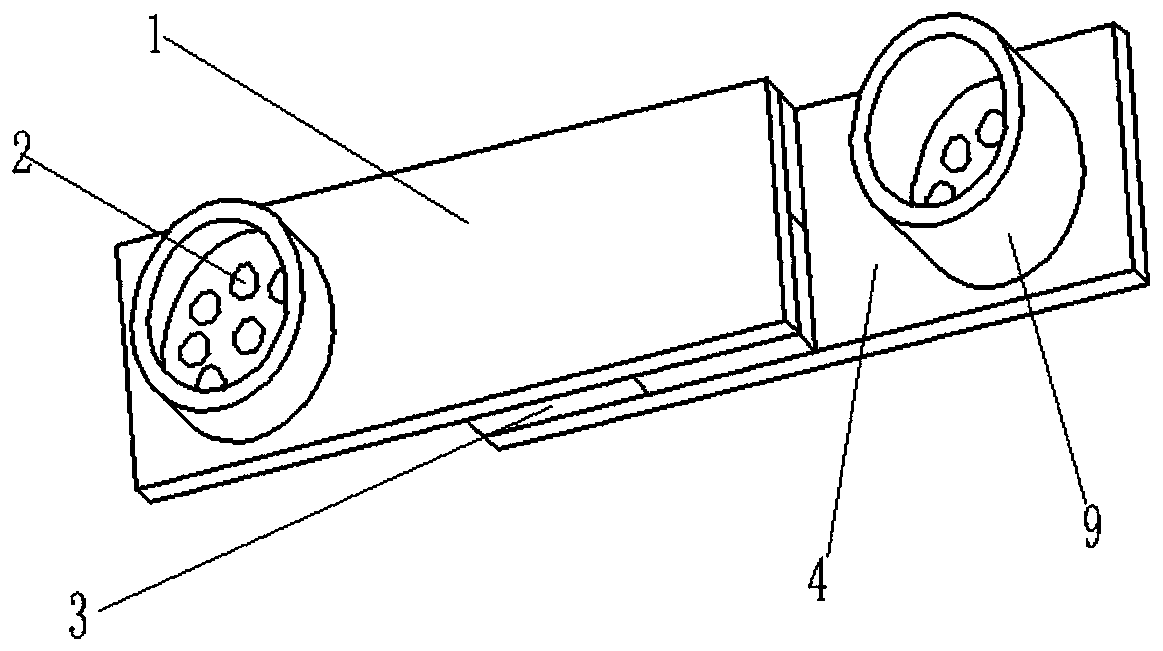
[0119] see figure 2 , based on the heat transfer device provided by the first embodiment of the present invention, the second embodiment of the present invention provides another heat transfer device, the difference is:
[0120] The heat transfer device further includes a guide tube 9 , the guide tube 9 is arranged on the heat conduction plate 1 , and the guide tube 9 is arranged around the fluid channel 2 . In this embodiment, the number of the semiconductor wafers 3 is four.
[0121] Heat insulating material may be filled between the two heat conducting plates 1 and between the two guide tubes 9 to prevent loss of heat and cold.
no. 3 example
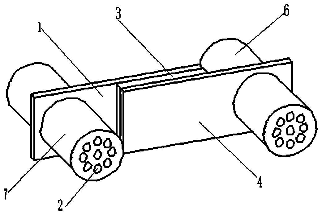
[0123] see image 3 , a heat transfer device based on a semiconductor wafer, comprising a semiconductor wafer 3 and two heat conduction plates 1, the semiconductor wafer 3 being sandwiched between the two heat conduction plates 1;
[0124] The heat transfer device 21 also includes two guide posts 6, the two guide posts 6 are respectively arranged on the two heat conduction plates 1, and the fluid guide posts 6 are provided with the fluid channel 2;
[0125] The semiconductor wafer 3 is located between the two fluid channels 2; the two fluid channels 2 respectively pass through two fluids with a temperature difference and opposite flow directions;
[0126] Wherein, the electric arm at the first end of the semiconductor wafer 3 and the electric arm at the second end are connected to a DC power supply device, so as to realize heat transfer between the first end surface and the second end surface of the semiconductor wafer 3;
[0127] Alternatively, the electrical arm at the fir...
PUM
 Abstract
Description
Claims
Application Information
 - R&D Engineer
- R&D Manager
- IP Professional
- Industry Leading Data Capabilities
- Powerful AI technology
- Patent DNA Extraction
Browse by: Latest US Patents, China's latest patents, Technical Efficacy Thesaurus, Application Domain, Technology Topic, Popular Technical Reports.
© 2024 PatSnap. All rights reserved.Legal|Privacy policy|Modern Slavery Act Transparency Statement|Sitemap|About US| Contact US: help@patsnap.com