Method for identifying nano plastic particles in aqueous solution based on scanning electron microscope-Raman technology
A nano-plastic and technical identification technology, applied in the field of nano-plastic identification, can solve the problems of easily damaged sample organic components, high electron beam energy and Raman light intensity, and achieve the effects of short time consumption, reduced background and improved quality.
- Summary
- Abstract
- Description
- Claims
- Application Information
AI Technical Summary
Problems solved by technology
Method used
Image
Examples
Embodiment 1
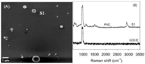
[0018] In-situ identification of standard nanoplastic particles in deionized aqueous solution of embodiment 1
[0019] First conduct a blank experiment, stick a clean silicon wafer to the metal substrate of the scanning electron microscope, then put it into the electron microscope for direct observation, and move it to the Raman spectrum, choose a point to measure according to the set experimental parameters, and get The Raman signal of the silicon wafer is used as a reference for subsequent tests.
[0020] A colloid solution containing standard polyvinyl chloride nanoplastic particles was dropped on a silicon wafer, and allowed to stand for 24 hours at room temperature to air-dry naturally. Before the measurement, stick the silicon chip with polyvinyl chloride nano-plastic particles on the metal substrate of the scanning electron microscope, and put it into the electron microscope for direct observation; after confirming the nano-plastic particles that need to be analyzed b...
Embodiment 2
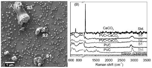
[0022] The identification of nanoparticles in embodiment 2 mineral water solution
[0023] Carry out a blank experiment first, stick a clean silicon wafer to the metal substrate of the scanning electron microscope, then put it into the electron microscope for direct observation, and move it to the Raman spectrum, choose a point to measure according to the set test parameters, and get The Raman signal of the silicon wafer is used as a reference for subsequent tests. The Raman spectrum of the silicon substrate is shown in figure 2 B, given the silicon substrate 960cm -1 The intensity of the Raman peak is too large, which will affect the display of other peaks, so the 960cm -1 Raman Peak is hidden.
[0024] Use 10 μm and 1 μm polyethersulfone filter membranes to sequentially filter the mineral water solution that may contain nanoparticles, and finally obtain an aqueous solution containing nanoparticles (<1 μm), drop the aqueous solution containing nanoparticles on a silicon...
Embodiment 3
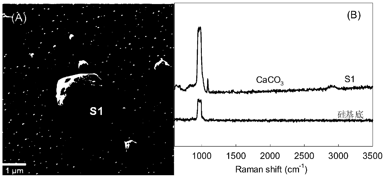
[0026] The identification of nanoparticles in the seawater solution of embodiment 3
[0027] First conduct a blank experiment, stick a clean silicon wafer to the metal substrate of the scanning electron microscope, then put it into the electron microscope for direct observation, and move it to the Raman spectrum, choose a point to measure according to the set test parameters, and get The Raman signal of the silicon wafer is used as a reference for subsequent tests. Use 10 μm and 1 μm polyethersulfone filter membranes to sequentially filter the aqueous solution that may contain nanoparticles, and finally obtain a seawater solution containing nanoparticles (<1 μm), drop the seawater solution containing nanoparticles on a silicon chip, and statically Let it dry naturally at room temperature for 24 hours.
[0028] Before the measurement, stick the silicon wafer containing the sample on the metal substrate of the scanning electron microscope, and then put it into the electron mi...
PUM
| Property | Measurement | Unit |
|---|---|---|
| particle diameter | aaaaa | aaaaa |
Abstract
Description
Claims
Application Information
 - Generate Ideas
- Intellectual Property
- Life Sciences
- Materials
- Tech Scout
- Unparalleled Data Quality
- Higher Quality Content
- 60% Fewer Hallucinations
Browse by: Latest US Patents, China's latest patents, Technical Efficacy Thesaurus, Application Domain, Technology Topic, Popular Technical Reports.
© 2025 PatSnap. All rights reserved.Legal|Privacy policy|Modern Slavery Act Transparency Statement|Sitemap|About US| Contact US: help@patsnap.com


