A method for igzo photocurrent regulation based on two-dimensional black phosphorus materials
A technology of black phosphorus and construction method, applied in circuits, electrical components, sustainable manufacturing/processing, etc., can solve the problems of complex preparation process of heterojunction devices, small sample size, and unstable device performance, etc., and achieve photocurrent intensity. and response time efficient, repeatable and easy to achieve
- Summary
- Abstract
- Description
- Claims
- Application Information
AI Technical Summary
Problems solved by technology
Method used
Image
Examples
Embodiment 1
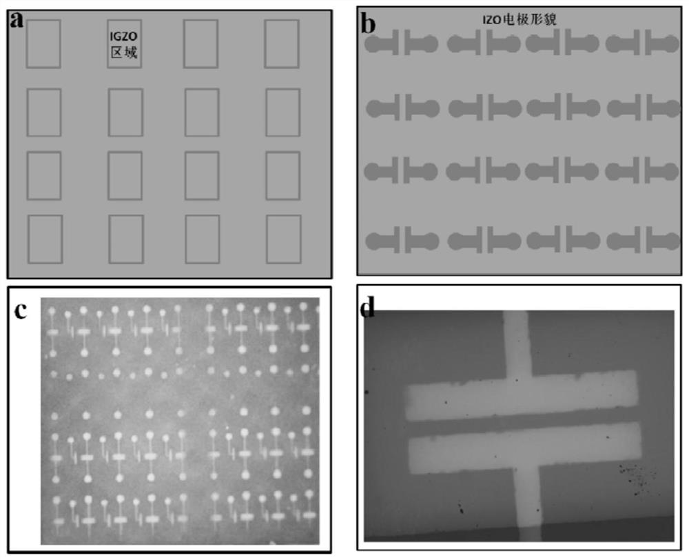
[0060] based on figure 1 The IGZO device is prepared using a mask, and the preparation process includes the following steps:
[0061] (1) Prepare the mask plate: draw the mask plate according to the needs of the experiment (such as figure 1 (a) and (b)), what used in the present embodiment is a set of mask plate, wherein a kind of is used for preparing IGZO channel layer (mask plate 1), and another kind is used for preparing electrode on IGZO surface (Mask version II), the channel width of mask version I is 40um, look for the mask version preparation manufacturer to process (the manufacturer that is looking for in this embodiment is micro-nano scientific research experiment equipment company), in order to guarantee the mask version Flatness and thinner thickness, the original material used is a stainless steel plate with a thickness of 3mm;
[0062] (2) Substrate cleaning: In this embodiment, a silicon wafer coated with a 300nm silicon dioxide layer is used as a substrate, a...
Embodiment 2
[0079] Embodiment 2 Change IGZO channel width
[0080] Prepare IGZO devices using a mask:
[0081] (1) Prepare mask plate: different from the mask plate in embodiment 1, the channel width of mask plate 1 in the present embodiment is 80um; Material and processing factory are all the same;
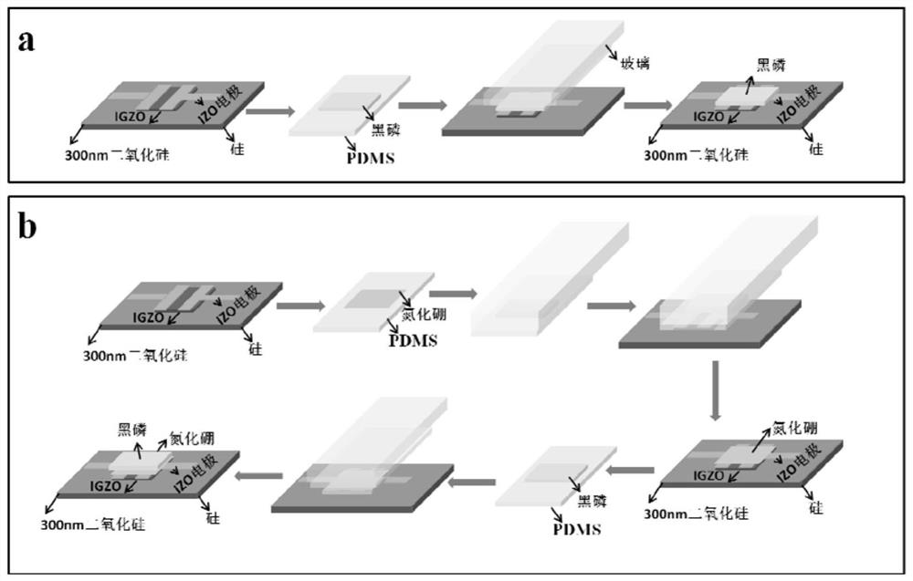
[0082] (2)~(5): Same as (2)~(5) in Example 1, prepare an IGZO device with a channel width of 80um; prepare black phosphorus-IGZO heterogeneous structures with different structures: same as in Example 1 The same preparation method, prepared four types of black phosphorus-IGZO heterogeneous.
[0083] Characterization of photocurrent performance of different types of heterojunctions (type I and type III): the photocurrent was measured by the test method in Example 1.
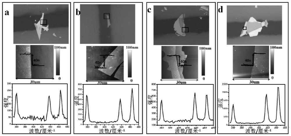
[0084] Test results such as Image 6 : In type I, that is, after the black phosphorus covers the electrodes at both ends of the channel, the photocurrent in the original IGZO decreases, but the magnitude of the decrease is not...
Embodiment 3
[0085] Embodiment 3 Changing the thickness of the IGZO channel
[0086] (1)~(2): same as (1)~(2) in embodiment 1;
[0087] (3) Use the fixture to fix the stainless steel mask on the pre-cut substrate surface with the same size as the mask. By controlling the fixture, the mask is in close contact with the substrate to avoid the magnetron sputtering process. Infiltrated IGZO; use magnetron sputtering method to deposit IGZO, put the substrate with fixed mask plate into the magnetron sputtering chamber, vacuumize to below 10Pa, and then pass in argon and oxygen, the flow rates are respectively 10mL / min and 0.3mL / min, the reaction pressure is 400mPa, the sputtering power is 1.76W / cm 2 , the sputtering time is 12min; a 40nm IGZO channel is prepared;
[0088] (4) to (5): Same as in Example 1.
[0089] Preparation of black phosphorus-IGZO heterojunctions with different structures: the same preparation method as in Example 1, to prepare type I and type III black phosphorus-IGZO hete...
PUM
| Property | Measurement | Unit |
|---|---|---|
| thickness | aaaaa | aaaaa |
| thickness | aaaaa | aaaaa |
| band gap | aaaaa | aaaaa |
Abstract
Description
Claims
Application Information
 - R&D
- Intellectual Property
- Life Sciences
- Materials
- Tech Scout
- Unparalleled Data Quality
- Higher Quality Content
- 60% Fewer Hallucinations
Browse by: Latest US Patents, China's latest patents, Technical Efficacy Thesaurus, Application Domain, Technology Topic, Popular Technical Reports.
© 2025 PatSnap. All rights reserved.Legal|Privacy policy|Modern Slavery Act Transparency Statement|Sitemap|About US| Contact US: help@patsnap.com


