A thin film preparation method of a quasi-one-dimensional structure material with controllable orientation
A technology for film preparation and dimensional structure, which is applied in sustainable manufacturing/processing, metal material coating process, final product manufacturing, etc., can solve the problem of uncontrollable quasi-one-dimensional material orientation, achieve simple and reliable adjustment methods, and reduce costs , the effect of good application potential
- Summary
- Abstract
- Description
- Claims
- Application Information
AI Technical Summary
Problems solved by technology
Method used
Image
Examples
preparation example Construction
[0039] Taking the substrate to be deposited below as an example on the substrate where an N-type buffer layer of a thin film solar cell has been deposited, the preparation method of the present invention comprises the following steps:
[0040] 1) Set as figure 1 The evaporation tube furnace shown.
[0041] 2) Preparation of substrate required for deposition of semiconductor thin film. For example, CdS thin films, ZnO thin films, TiO 2 Thin film and other common thin film solar cell N-type buffer layer to obtain the substrate to be deposited.
[0042] 3) Weigh 0.2g-0.3g material powder and sieve it with a 50-mesh sieve and put it into the crucible as the evaporation source, shake it gently to spread the powder on the bottom of the crucible, and then put the evaporation source in the middle of the heating area of the tube furnace . The crucible can be a quartz crucible with a diameter of 8-15mm. The evaporation source is an anisotropic quasi-one-dimensional material, such...
Embodiment 1
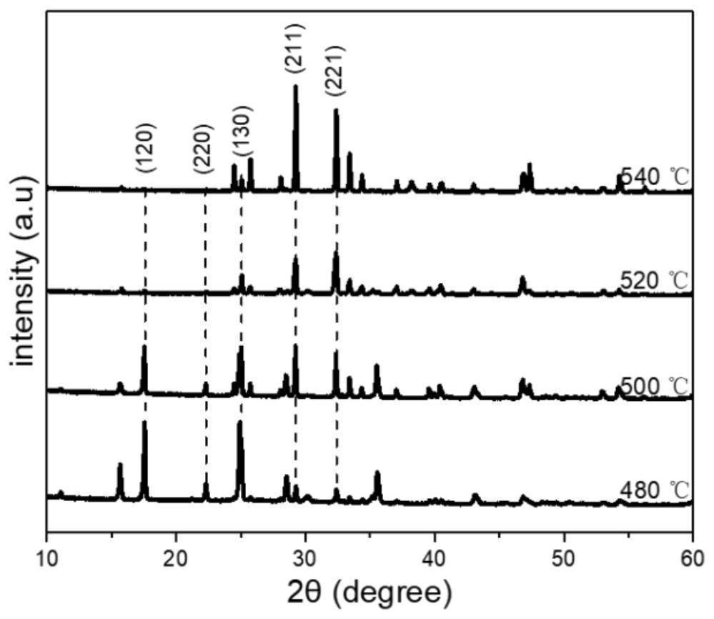
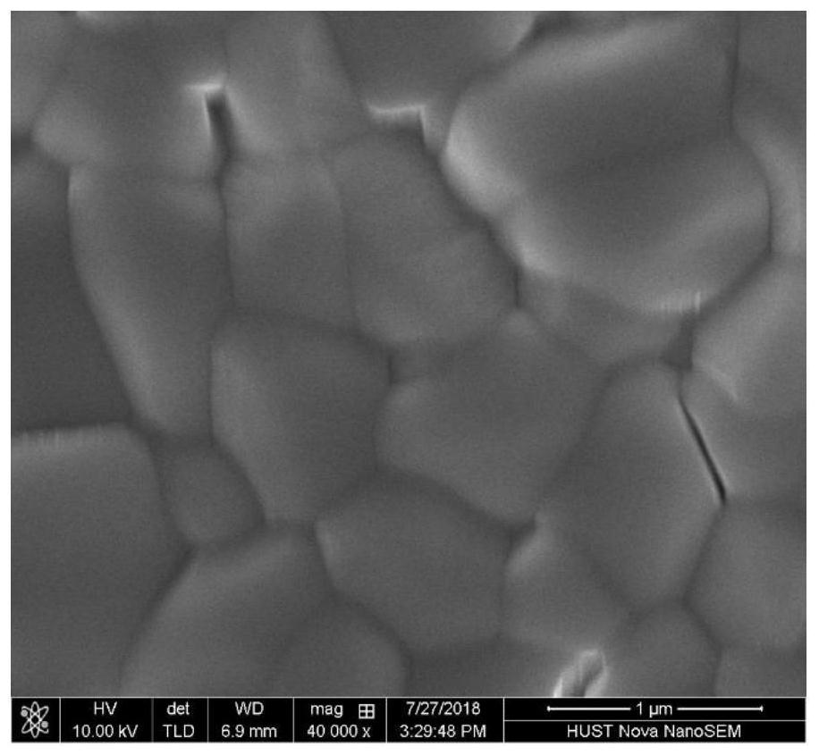
[0048] Embodiment 1: Orientation modulation of different antimony sulfide absorption layers
[0049] (1) Cut the ITO conductive glass into a size of 5cm×5cm, respectively use detergent, isopropanol and absolute ethanol to ultrasonically clean it for 30min, and then dry it with nitrogen for later use.
[0050] (2) Preparation of substrate: Deposit cadmium sulfide on the washed ITO with a thickness of about 50 nm by using a chemical water bath method. Specifically, pour 220mL of deionized water, 30mL of 0.05mol / L cadmium sulfate solution and 39.3mL of 25% ammonia water into the beaker, and stir at 67°C for 3 minutes, then add 15mL of 1.5mol / L The thiourea was poured in, and the ITO conductive glass was put in at the same time, and the constant temperature was reacted for 16 minutes. After the reaction, take it out and dry it with nitrogen gas to obtain a cadmium sulfide substrate.
[0051] (3) Weighing of evaporation source: Weigh 0.2g of antimony sulfide powder with a purity ...
Embodiment 2
[0060] Example 2: Orientation Modulation of Vertical Bismuth Sulfide Absorbing Layer
[0061] (1) Cut the ITO conductive glass into a size of 5cm×5cm, respectively use detergent, isopropanol and absolute ethanol to ultrasonically clean it for 30min, and then dry it with nitrogen for later use.
[0062] (2) Preparation of substrate: This step is the same as step (2) in Example 1.
[0063] (3) Selection of evaporation source: Weighing 0.2g of 98% bismuth sulfide powder with a purity of 0.2g is finely screened with a 50-mesh sieve and placed in a quartz crucible with a bottom diameter of 12mm. The crucible is placed in the middle of the quartz tube heating zone using a stainless steel shelf. .
[0064] (4) Purification of powder: set the heating program, raise it to 630°C at 16°C / min, put the substrate into air steam, and purify once. After the program is finished, open the lid and let it cool down to room temperature naturally.
[0065] (5) Preparation of film: such as figur...
PUM
| Property | Measurement | Unit |
|---|---|---|
| diameter | aaaaa | aaaaa |
| thickness | aaaaa | aaaaa |
Abstract
Description
Claims
Application Information
 - R&D
- Intellectual Property
- Life Sciences
- Materials
- Tech Scout
- Unparalleled Data Quality
- Higher Quality Content
- 60% Fewer Hallucinations
Browse by: Latest US Patents, China's latest patents, Technical Efficacy Thesaurus, Application Domain, Technology Topic, Popular Technical Reports.
© 2025 PatSnap. All rights reserved.Legal|Privacy policy|Modern Slavery Act Transparency Statement|Sitemap|About US| Contact US: help@patsnap.com


