
LED epitaxial growth method taking graphene as buffer layer

A technology of epitaxial growth and buffer layer, applied in the direction of electrical components, circuits, semiconductor devices, etc., can solve problems such as difficult stripping, limited application, lattice mismatch, etc., to reduce the difficulty of stripping, reduce production costs, and reduce dependence Effect

Inactive Publication Date: 2020-04-10
XIANGNENG HUALEI OPTOELECTRONICS
View PDF5 Cites 1 Cited by
  • Summary
  • Abstract
  • Description
  • Claims
  • Application Information

AI Technical Summary

Problems solved by technology

[0002] A light-emitting diode (Light-Emitting Diode, LED) is a semiconductor electronic device that converts electrical energy into light energy. Among them, LED products made of gallium nitride are subject to the traditional buffer layer preparation method (growing nitride directly on the substrate gallium materials), gallium nitride materials are mostly on high-quality crystal substrates (such as sapphire, silicon and silicon carbide, etc.) to obtain LED products through metal chemical vapor deposition method MOCVD epitaxy. The following shortcomings: 1) The available epitaxial area of ​​high-quality crystal substrates is small, which limits the growth area of ​​GaN epitaxial layers, and cannot meet the preparation of large-area GaN epitaxial layers, which in turn limits the use of GaN LED products in flexible displays, Applications in smart wearable devices, etc.; 2) Strong bonding between GaN epitaxial layers and high-quality crystal substrates, making it difficult to peel off LED products made of GaN from substrates; 3) High-quality crystals Substrates are expensive, increasing production costs
However, since the quartz glass substrate is an amorphous material, there is a problem of lattice mismatch between it and the GaN epitaxial layer, and the preparation of a large-area GaN epitaxial layer cannot be realized, which limits the use of GaN LED products in flexible displays. , smart wearable devices, and other applications. In addition, using traditional buffer layer preparation methods to epitaxial GaN layers on amorphous substrates cannot solve the problem of difficult peeling between LED products and substrates.
[0004] To sum up, there is an urgent need for an LED epitaxial growth method using graphene as a buffer layer to solve the problem that the existing LED products using GaN as the material cannot realize the preparation of large-area GaN epitaxial layers and the difficulty of peeling off from the substrate big problem

Method used


Image

  • LED epitaxial growth method taking graphene as buffer layer
  • LED epitaxial growth method taking graphene as buffer layer
  • LED epitaxial growth method taking graphene as buffer layer

Examples


Embodiment 1

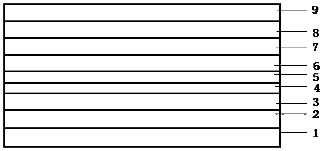
[0038] see figure 1 , a method for epitaxial growth of LEDs using graphene as a buffer layer, comprising the process of growing a graphene buffer layer 2 and an aluminum nitride layer 3 in sequence, specifically:

[0039] Step 1, growing a graphene buffer layer 2 on the substrate 1;

[0040] Step 2, growing an aluminum nitride layer 3 on the graphene buffer layer 2.

[0041] Described step 1 comprises the following steps:

[0042] Step 1.1, preparing the graphene buffer layer 2 separately, specifically: using chemical vapor deposition method, using methane as the carbon source, using copper foil as the substrate, placing the copper foil in a quartz tube, and the quartz tube is placed in a resistance furnace, sealed Quartz tube, heat up to 930-1100°C and keep it for 60-100 minutes, pass in argon gas with a flow rate of 150-200mL / min and keep it for 10-30 minutes, perform high-temperature preheating treatment on copper foil, and pass in a flow rate of 10-20mL / min Min of metha...


PUM

PropertyMeasurementUnit
quality scoreaaaaaaaaaa

Abstract

The invention provides an LED epitaxial growth method taking graphene as a buffer layer. The LED epitaxial growth method comprises the following steps: 1, growing a graphene buffer layer on a substrate; 2, growing an aluminum nitride layer on the graphene buffer layer; 3, processing the composite substrate; 4, growing an aluminum gallium nitride layer; 5, growing an undoped gallium nitride layer;6, growing a silicon-doped N-type gallium nitride layer; 7, growing a light-emitting layer; 8, growing a P-type aluminum gallium nitride layer doped with aluminum and magnesium; 9, growing a P-type gallium nitride layer doped with magnesium; and 10, carrying out heat preservation for 20-30 minutes at the temperature of 650-680 DEG C, closing the heating system and the gas supply system, and carrying out furnace cooling. The epitaxial growth method provided by the invention can effectively solve the problems of preparation of a large-area gallium nitride epitaxial layer and high stripping difficulty between the epitaxial layer and the substrate.

Description

technical field [0001] The invention relates to the technical field of LEDs, in particular to an LED epitaxial growth method using graphene as a buffer layer. Background technique [0002] A light-emitting diode (Light-Emitting Diode, LED) is a semiconductor electronic device that converts electrical energy into light energy. Among them, LED products made of gallium nitride are subject to the traditional buffer layer preparation method (growing nitride directly on the substrate gallium materials), gallium nitride materials are mostly on high-quality crystal substrates (such as sapphire, silicon and silicon carbide, etc.) to obtain LED products through metal chemical vapor deposition method MOCVD epitaxy. The following shortcomings: 1) The available epitaxial area of ​​high-quality crystal substrates is small, which limits the growth area of ​​GaN epitaxial layers, and cannot meet the preparation of large-area GaN epitaxial layers, which in turn limits the use of GaN LED prod...

Claims


Application Information

Patent Timeline
Patent Type & Authority Applications(China)
IPC IPC(8): H01L33/00H01L33/12
CPCH01L33/007H01L33/12
Inventor 梁萌刘志强伊晓燕苗振林周佐华季辉王良臣王军喜李晋闽
Owner XIANGNENG HUALEI OPTOELECTRONICS
Learn More