3D switching type PCB and manufacturing method thereof

The technology of a kind of PCB board and manufacturing method is applied in the field of 3D transfer type PCB board and its production, which can solve the problems of inability to make transfer type PCB board, unreasonable design of transfer type PCB board, and difficulty in manufacturing, etc., and achieve reduction Wick effect, avoid burrs, easy to control the effect

Active Publication Date: 2020-03-20
VICTORY GIANT TECH HUIZHOU CO LTD
View PDF7 Cites 1 Cited by
  • Summary
  • Abstract
  • Description
  • Claims
  • Application Information

AI Technical Summary

Problems solved by technology

[0004] In order to solve the problems of the unreasonable design of the existing transfer PCB board, the difficulty in production, and the inability to produce a transfer PCB board that meets the conditions of use, a set of A kind of 3D transfer type PCB board and preparation method thereof

Method used


Image

  • 3D switching type PCB and manufacturing method thereof
  • 3D switching type PCB and manufacturing method thereof
  • 3D switching type PCB and manufacturing method thereof

Examples


Embodiment Construction

[0032] The present invention will be further elaborated below in conjunction with the accompanying drawings and embodiments.

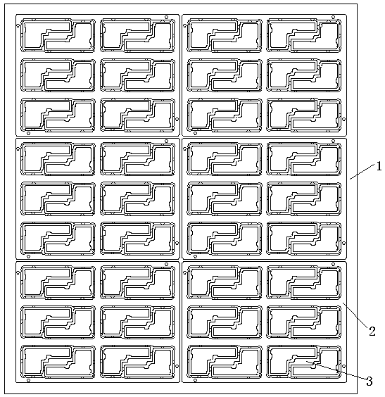
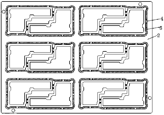
[0033] With reference to the accompanying drawings, a 3D transfer PCB board includes a PNL board 1 and a PCB board 3 located on the PNL board. The PCB is provided with at least one inner groove 6, and the edge of the inner groove 6 is provided with Edge wrapping groove 5 and connection position 4, the connection position is used to connect between each inner groove, and between the inner groove and the PNL board. Reference attached figure 1 The PNL board is composed of 6 SET boards 2, each SET board includes 12 PCB boards, and each PCB board is provided with an inner groove 6.

[0034] A method for manufacturing a 3D transfer type PCB board, the PNL board is followed by the following steps:

[0035] S1: Carry out cutting, baking, copper reduction and drilling on the PNL board in sequence. PNL board cutting substrate is made of high TG and CAF-resist...


PUM


Abstract

The invention discloses a 3D switching type PCB. The circuit board comprises a PNL board and a PCB arranged on the PNL board. The PCB is provided with at least one inner groove, the edge of each innergroove is provided with an edge covering groove and a connecting position, the connecting positions are used for connecting the inner grooves and connecting the inner grooves and the PNL board, the PCB is reasonable in design, the edge covering grooves can reduce board edge radiation interference, and transmission of high-speed signals is guaranteed. The invention further provides a manufacturingmethod of the 3D switching type PCB, all the steps are easy to control, the problems of burrs and burrs of the edge covering groove are effectively avoided, the precision of the sizes and positions of the edge covering groove and the inner groove is improved, and the reliability of long-term use of a product is improved.

Description

technical field [0001] The invention relates to the field of PCB boards, in particular to a 3D transfer type PCB board and a manufacturing method thereof. Background technique [0002] Today, when battery technology has not yet made a major breakthrough, increasing the battery capacity is the most direct and effective way to obtain a longer mobile phone battery life. How to accommodate a larger capacity battery without increasing the size of the mobile phone has become a dilemma A big problem facing R&D engineers. At present, there is a new "stacked" motherboard technology, using an interposer (a kind of adapter board) to tightly package the motherboard and chips together in layers, so that it takes up less space and can reduce the motherboard area by about 40%. Leave more space inside the mobile phone to accommodate larger batteries and bring better battery life. InterposerPCB, as an interposer transfer board, plays a linking role. It needs to have excellent three-way dens...

Claims


Application Information

Patent Timeline
Patent Type & Authority Applications(China)
IPC IPC(8): H05K3/00H05K3/18
CPCH05K3/0052H05K3/188
Inventor 何艳球张亚锋蒋华张永谋叶锦群
Owner VICTORY GIANT TECH HUIZHOU CO LTD
Why Eureka
Try Eureka