Flexible label-free nano bulge metasurface structure and manufacturing and sensing methods thereof
A metasurface, label-free technology, applied in the field of biomedical detection, which can solve the problems of expensive patterning and time-consuming
- Summary
- Abstract
- Description
- Claims
- Application Information
AI Technical Summary
Problems solved by technology
Method used
Image
Examples
Embodiment 1
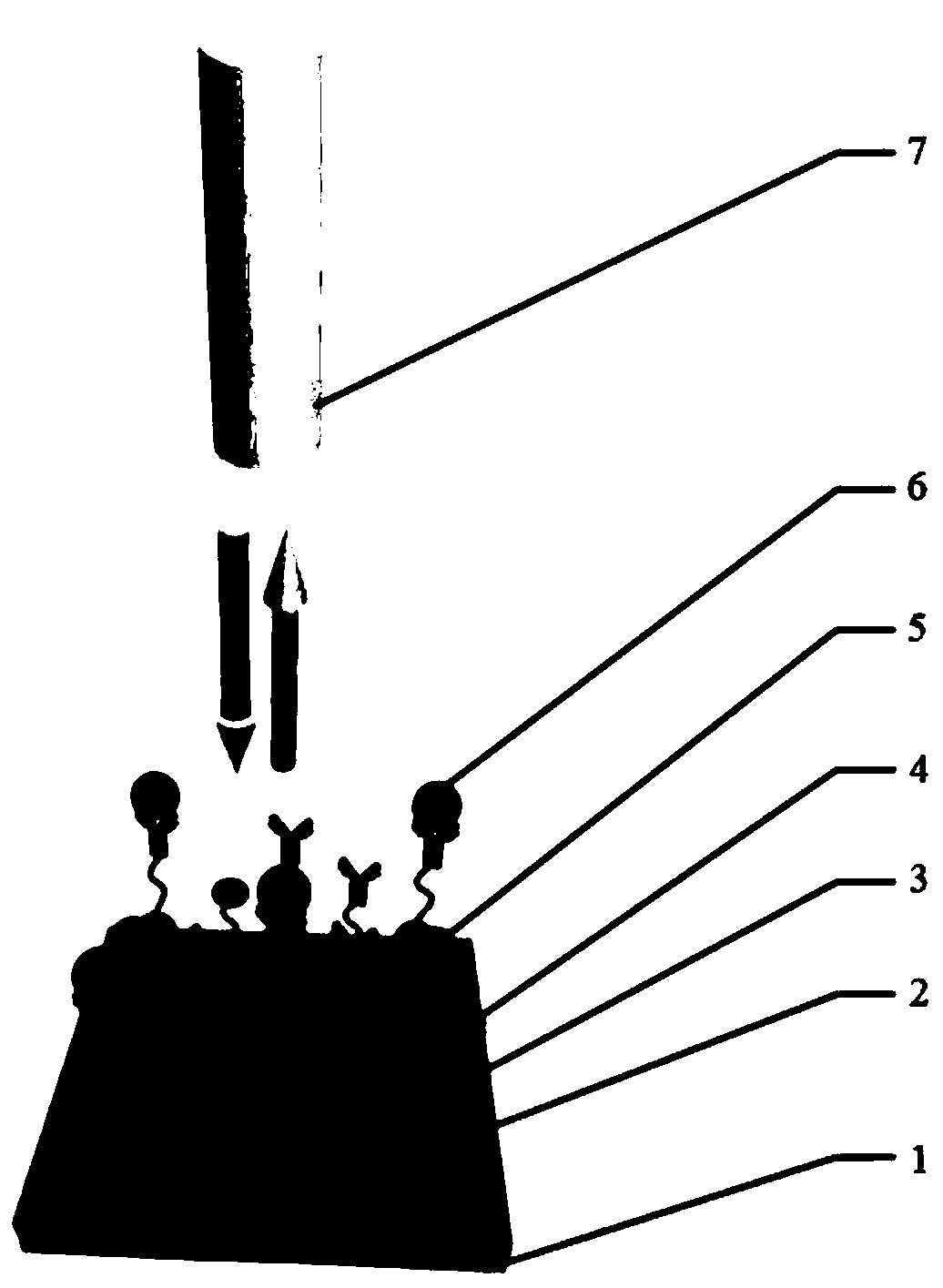
[0035] see figure 1 , the embodiment of the present invention provides a flexible label-free nano-protrusion metasurface structure (hereinafter referred to as the metasurface structure). The flexible label-free nano-protrusion metasurface structure includes: a metasurface structure chip (not marked), a biological reagent (not labeled) and integrated fiber optic probe (7).
[0036] In the embodiment of the present invention, the above-mentioned metasurface structure chip is composed of substrate (1), chromium film and gold film (2) sequentially from bottom to top, wherein, the substrate (1) is covered with nickel mold stamped Periodic array of nanopillars.
[0037] As a preferred embodiment of the present invention, the thickness of the chromium film in the chromium film and the gold film (2) is 5 nm, and the thickness of the gold film is 150 nm.
[0038] As another preferred embodiment of the present invention, the above-mentioned periodic nanopillar array has a diameter of ...
Embodiment 2
[0044] The embodiment of the present invention also provides a method for fabricating a flexible label-free nano-protrusion metasurface structure, comprising the following steps:
[0045]The first step: nanoimprinting, under the pressure of 40bar, within the temperature range of 110°C to 150°C, the substrate (1) is heat-treated with a 2-inch nickel mold to form a periodic nanopillar array.
[0046] The second step: plasma etching, setting different etching times, etching the periodic nano-column array in the nano-imprinting step with oxygen plasma, and etching the nano-column array into a nano-protrusion substrate.
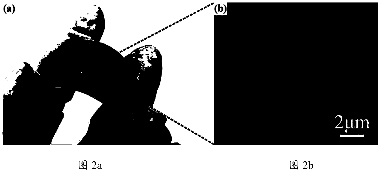
[0047] As a preferred embodiment of the present invention, the optimal etching time in the above-mentioned plasma etching step is 425s, it can be seen that the diameter and shape of the nano-column array of the surface structure will change at this time (see specifically image 3 ), which can reduce the reflectivity at the optimal etching time, and also show chara...
Embodiment 3
[0053] The embodiment of the present invention also provides a sensing method for a flexible label-free nano-protrusion metasurface structure, comprising the following steps:
[0054] Step 1: Prepare a 10 mmol / L MUA ethanol solution, and store the supersurface structure in the MUA ethanol solution for 8 to 14 hours to form a MUA self-assembled film.
[0055] As a preferred embodiment of the present invention, the above storage time is 12 hours.
[0056] Step 2: Prepare the EDC solution of 400mmol / L and the NHS solution of 100mmol / L, first clean the metasurface structure in the above step 1 with deionized water, then use the EDC solution of 400mmol / L and the NHS solution of 100mmol / L to dissolve the supersurface structure Surface structures were soaked for 0.5 h to activate MUA (3).
[0057] Step 3: soak the metasurface structure in the above step 2 in 40ug / mL CEA antibody solution for 0.5 to 1.5 hours, so that the CEA antibody in the CEA antibody solution binds to the MUA (3)...
PUM
| Property | Measurement | Unit |
|---|---|---|
| Thickness | aaaaa | aaaaa |
| Thickness | aaaaa | aaaaa |
Abstract
Description
Claims
Application Information
 - R&D
- Intellectual Property
- Life Sciences
- Materials
- Tech Scout
- Unparalleled Data Quality
- Higher Quality Content
- 60% Fewer Hallucinations
Browse by: Latest US Patents, China's latest patents, Technical Efficacy Thesaurus, Application Domain, Technology Topic, Popular Technical Reports.
© 2025 PatSnap. All rights reserved.Legal|Privacy policy|Modern Slavery Act Transparency Statement|Sitemap|About US| Contact US: help@patsnap.com


