Reaction chamber and semiconductor processing equipment

A technology of reaction chamber and process position, which is applied in the direction of semiconductor/solid-state device manufacturing, discharge tube, electrical components, etc., can solve the problems of increasing cleaning steps, affecting the process effect, falling on the surface of the substrate, etc., to achieve process capacity and process The effect is improved, the etching rate and uniformity are improved, and the effect of preventing the generation of pollutants

Pending Publication Date: 2020-02-21
BEIJING NAURA MICROELECTRONICS EQUIP CO LTD
View PDF5 Cites 2 Cited by
  • Summary
  • Abstract
  • Description
  • Claims
  • Application Information

AI Technical Summary

Problems solved by technology

[0004] However, when the ions produced by the process gas under the action of the electric field bombard the surface of the substrate, they will also bombard the metal surface outside the groove on the metal tray 14, and the metal particles produced will fall on the surface of the substrate to form new pollutants.
For this reason, it is also necessary to increase the cleaning step to bombard the newly formed contaminants, resulting in a decrease in the etching rate of the pre-cleaning process and affecting the process throughput
In addition, there are more metal particles falling near the edge of the substrate than metal ions falling on the center of the substrate, which will reduce the etching uniformity of the pre-cleaning process and affect the process effect

Method used


Image

  • Reaction chamber and semiconductor processing equipment
  • Reaction chamber and semiconductor processing equipment
  • Reaction chamber and semiconductor processing equipment

Examples


Embodiment Construction

[0028] In order for those skilled in the art to better understand the technical solution of the present invention, the reaction chamber and semiconductor processing equipment provided by the present invention will be described in detail below in conjunction with the accompanying drawings.

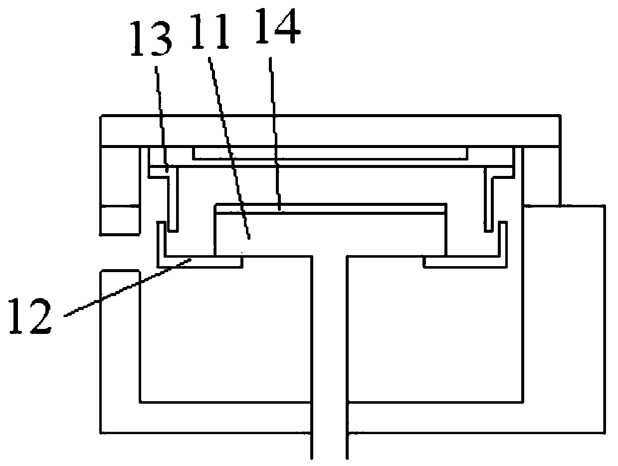
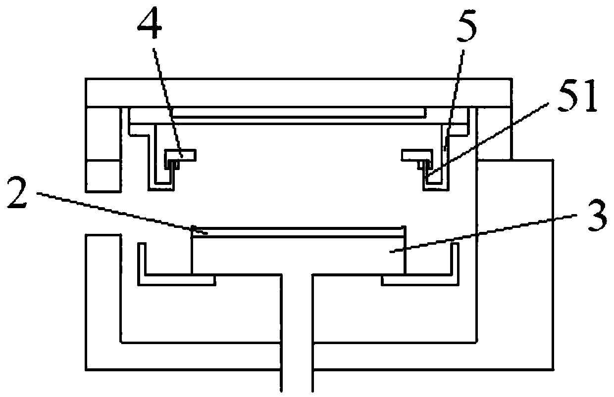
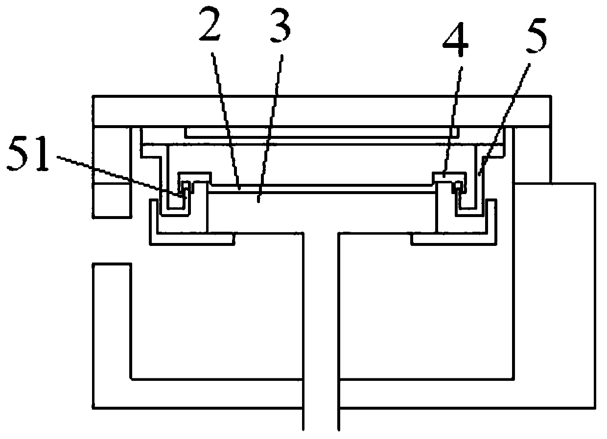
[0029] Such as Figure 2-Figure 6 As shown, this embodiment provides a reaction chamber, including a base 3, a tray 2 carried on the base 3, a cover plate 4 and a liner 5, wherein the base 3 is liftable and can be lowered Go to the pick-up position to pick and place the tray 2, or go up to the process position for process. The tray 2 can be moved into or out of the reaction chamber, and includes a bearing position for carrying the substrate, the shape and size of the bearing position are consistent with the substrate, the cover plate 4 is used to cover the area of ​​the tray 2 except the bearing position, and the inner lining 5 is arranged around the inside of the side wall of the reaction...


PUM

PropertyMeasurementUnit
thicknessaaaaaaaaaa
depthaaaaaaaaaa
thicknessaaaaaaaaaa

Abstract

The invention provides a reaction chamber and semiconductor processing equipment, and the reaction chamber comprises a substrate, a tray borne on the substrate, a cover plate and a lining. The tray comprises a bearing position for bearing the substrate, and the cover plate is used for covering the area, except the bearing position, of the tray. The lining is arranged around the inner side of the side wall of the reaction chamber, a supporting part is arranged on the lining, and the supporting part is used for supporting the cover plate to separate the cover plate from the tray when the substrate descends from the process position. According to the reaction chamber provided by the invention, ions generated by process gas can be prevented from bombarding the tray, and pollutants are prevented from being generated, so that the etching rate and uniformity of pre-cleaning are improved, and the process capacity and process effect are improved.

Description

technical field [0001] The present invention relates to the technical field of semiconductor process equipment, in particular, to a reaction chamber and semiconductor processing equipment. Background technique [0002] At present, in the semiconductor process, the substrate (Wafer) generally needs to be pre-cleaned (Preclean) before the film growth process to remove the pollutants on the surface of the substrate to ensure that the subsequent growth of the film has better adhesion. The core indicators of the pre-cleaning process are etching rate, uniformity and selectivity ratio. Capacitively Coupled Plasma Preclean (CCP Preclean, Capacitively Coupled Plasmas Preclean) is a common equipment for the pre-cleaning process. [0003] Such as figure 1 As shown, an existing capacitively coupled plasma pre-cleaning device includes a base 11, a lower lining 12, an upper lining 13 and a metal tray 14, wherein the metal tray 14 is provided with a groove for placing a substrate, and Wh...

Claims


Application Information

Patent Timeline
Patent Type & Authority Applications(China)
IPC IPC(8): H01J37/32H01L21/67
CPCH01J37/32458H01J37/32853H01J37/32091H01L21/67017
Inventor 宋海洋赵磊王文章郭万国刘菲菲高晓丽
Owner BEIJING NAURA MICROELECTRONICS EQUIP CO LTD
Why Eureka
Try Eureka