MEMS structure and processing method thereof, pyroelectric sensor and infrared detector
A processing method and heat-sensitive technology, applied in the field of MEMS technology and infrared detection, can solve the problems of inapplicability, large noise equivalent temperature difference, and large influence on the overall performance of the detector.
- Summary
- Abstract
- Description
- Claims
- Application Information
AI Technical Summary
Problems solved by technology
Method used
Image


Examples
Embodiment 1
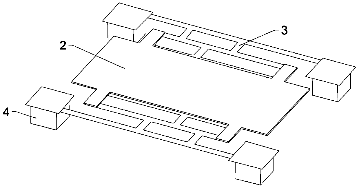
[0038] Refer to attached Figure 1~2 , this embodiment provides a MEMS structure, which includes a substrate 1 provided with a readout integrated circuit, a thermally sensitive layer 2 suspended on the upper side of the substrate 1, and a support structure 3 for supporting the thermally sensitive layer 2; The heat-sensitive layer 2 described above is a ferroelectric film of lead lanthanum titanate; the support structure is electrically connected to the substrate 1 through four groups of anchor columns 4, and an optical resonance is formed between the support structure 3 and the substrate 1 Cavity 7 ; the support structure 3 includes a first silicon carbide layer 31 , an electrode layer 32 and a second silicon carbide layer 33 sequentially from bottom to top.
[0039] Wherein, the electrode layer 32 is an interdigitated electrode structure, and the anchor column 4 is made of tungsten; the outer periphery of the anchor column 4 is provided with a silicon oxide layer 5, which can...
Embodiment 2
[0041] Refer to attached Figure 1~2 , this embodiment provides a method for processing the MEMS structure provided in the above-mentioned embodiment 1, which includes the following steps:
[0042] (1) Spin-coat a polyimide film with a thickness of 1 μm on the substrate 1 as a sacrificial layer, and deposit a silicon carbide protective film on the sacrificial layer by chemical vapor deposition to protect the polyimide The role of the membrane.
[0043] (2) Etching and drilling the four corners of the sacrificial layer and the silicon carbide protective film to obtain four groups of first holes.
[0044] (3) Deposit silicon oxide in the above-mentioned first channel by chemical vapor deposition, and planarize the sacrificial layer for the first time, and remove the silicon carbide protective film on the sacrificial layer.
[0045] (4) Deposit a silicon oxynitride protective film with a thickness of 40 nm on the sacrificial layer after the first planarization by chemical vapor...
Embodiment 3
[0054] Refer to attached Figure 1~2 , this embodiment provides a method for processing the MEMS structure provided in the above-mentioned embodiment 1, which includes the following steps:
[0055] (1) Spin-coat a polyimide film with a thickness of 3 μm on the substrate 1 as a sacrificial layer, and deposit a silicon carbide protective film on the sacrificial layer by chemical vapor deposition to protect the polyimide The role of the membrane.
[0056] (2) Etching and drilling the four corners of the sacrificial layer and the silicon carbide protective film to obtain four groups of first holes.
[0057] (3) Deposit silicon oxide in the above-mentioned first channel by chemical vapor deposition, and planarize the sacrificial layer for the first time, and remove the silicon carbide protective film on the sacrificial layer.
[0058] (4) Deposit a silicon oxynitride protective film with a thickness of 40 nm on the sacrificial layer after the first planarization by chemical vapor d...
PUM
| Property | Measurement | Unit |
|---|---|---|
| Thickness | aaaaa | aaaaa |
| Thickness | aaaaa | aaaaa |
| Thickness | aaaaa | aaaaa |
Abstract
Description
Claims
Application Information
 - Generate Ideas
- Intellectual Property
- Life Sciences
- Materials
- Tech Scout
- Unparalleled Data Quality
- Higher Quality Content
- 60% Fewer Hallucinations
Browse by: Latest US Patents, China's latest patents, Technical Efficacy Thesaurus, Application Domain, Technology Topic, Popular Technical Reports.
© 2025 PatSnap. All rights reserved.Legal|Privacy policy|Modern Slavery Act Transparency Statement|Sitemap|About US| Contact US: help@patsnap.com