
Antimonide superlattice very-long wave infrared detector with dark current suppression structure

An infrared detector and super-lattice technology, applied in circuits, electrical components, semiconductor devices, etc., can solve the problem of low dynamic impedance, achieve the effect of improving dynamic impedance, dark current impedance, and comprehensive detection rate

Active Publication Date: 2020-02-14
NANJING UNIV
View PDF4 Cites 8 Cited by
  • Summary
  • Abstract
  • Description
  • Claims
  • Application Information

AI Technical Summary

Problems solved by technology

The problem with existing VLWIR detectors is that the dynamic impedance R 0 A is low and decreases rapidly with increasing reverse bias voltage

Method used


Image

  • Antimonide superlattice very-long wave infrared detector with dark current suppression structure
  • Antimonide superlattice very-long wave infrared detector with dark current suppression structure
  • Antimonide superlattice very-long wave infrared detector with dark current suppression structure

Examples


Embodiment Construction

[0059] In order to make the object, technical solution and advantages of the present invention clearer, the present invention will be described in further detail below in conjunction with specific embodiments and with reference to the accompanying drawings.

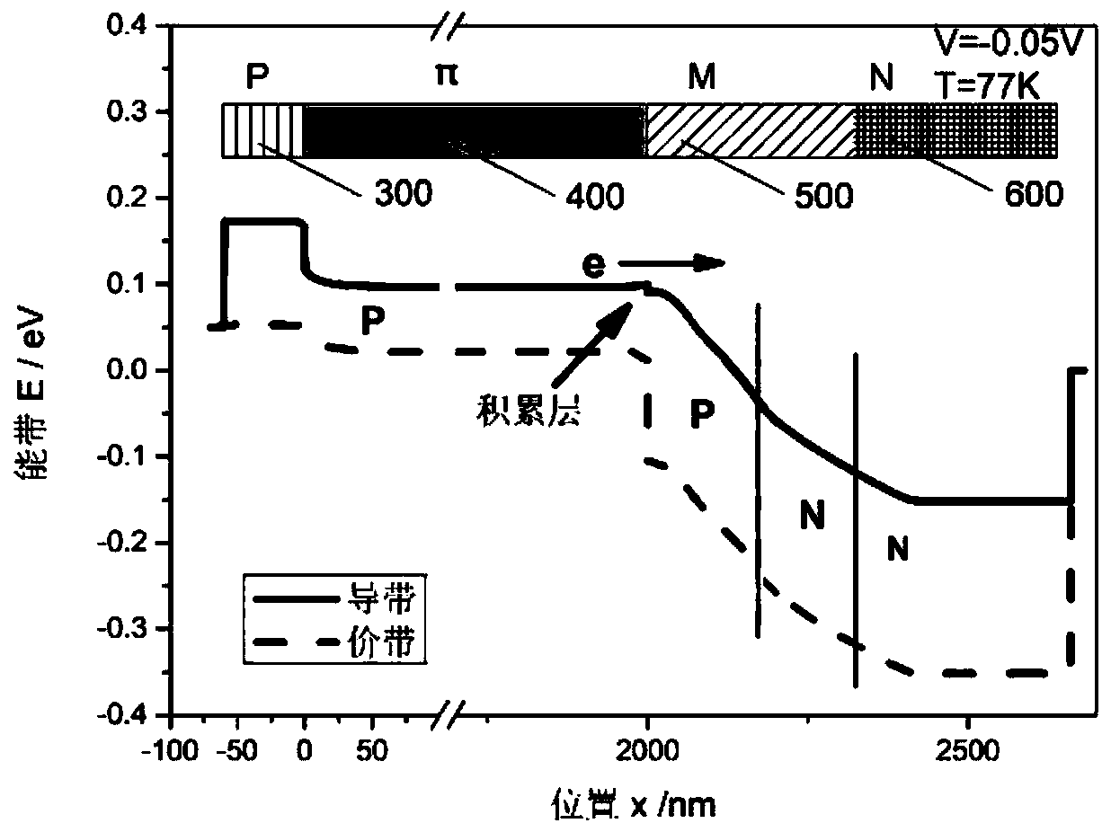
[0060] figure 1 Shown is a device structure diagram proposed according to the present invention, a P-type doped GaSb buffer layer 200 is sequentially grown on a semi-insulating GaSb substrate 100, a P-type doped InAs / GaSb mid-wave superlattice material contact P region 300, Absorption π region 400 of P-type doped InAs / GaSb very long-wave superlattice material, barrier M region 500 of P-type segmentally doped InAs / GaSb / AlSb superlattice material, N-type segmentally doped InAs / A contact N region 600 of GaSb / AlSb superlattice material, and an N-type doped InAs cap layer / contact layer 700 . In addition to the superlattice material, it also includes a passivation layer material 950 deposited on the material, and an upper ele...


PUM

PropertyMeasurementUnit
thicknessaaaaaaaaaa
thicknessaaaaaaaaaa

Abstract

The invention relates to an antimonide superlattice very-long wave infrared detector with a dark current suppression structure so as to suppress a device dark current and improve photon-generated carrier transport. The detector comprises a substrate, a buffer layer arranged on the substrate in an epitaxial manner, a medium-long wave band contact layer which is called as a P region and is arrangedon the buffer layer in an epitaxial manner, a very-long wave band absorption layer which is called as a pi region and is arranged on the P region of the medium-long wave band contact layer in an epitaxial manner, a medium-long wave band barrier layer which is called as an M region and is arranged on the pi region of the very-long wave band absorption layer in an epitaxial manner, a medium-long wave band contact layer which is called as an N region and is arranged on the medium-long wave band barrier layer M region in an epitaxial manner, and a cover layer arranged on an N region of the medium-long wave band contact layer in an epitaxial manner, wherein doping modes and thickness of the superlattice structure, the absorption layer and the barrier layer of each region are adjusted and controlled so as to design an energy band structure of the infrared detector. The detector is advantaged in that the detector is based on a PpiMN structure, and a brand-new barrier structure design is provided and relates to superlattice, thickness and doping.

Description

technical field [0001] The invention belongs to the technical field of semiconductor devices, and in particular relates to a structure of a superlattice very long-wave infrared detector to suppress device dark current and improve photogenerated carrier transport. Especially the energy band structure of a VLWIR detector based on antimonide superlattice. Based on the PπMN structure, the structure proposes a new barrier structure design involving superlattice structure, thickness and doping, etc. Background technique [0002] Objects above absolute zero are always radiating electromagnetic waves to the outside world, and those with wavelengths in the range of 0.76-1000 μm are called infrared radiation. Objects exhibit different infrared characteristics due to their different temperatures, so infrared detection technology has extensive and important applications in military, civilian, astronomical and other fields. Among them, the very long wave infrared detection technology (...

Claims


Application Information

Patent Timeline
Patent Type & Authority Applications(China)
IPC IPC(8): H01L31/0352H01L31/103
CPCH01L31/035263H01L31/035236H01L31/03529H01L31/1035
Inventor 岳壮豪施毅牛智川王国伟徐应强蒋洞微常发冉李勇
Owner NANJING UNIV
Learn More