A kind of LED containing pmot:ppv/zno:cu/zno:al heterojunction and its preparation method
A heterojunction and homojunction technology, applied in semiconductor/solid-state device manufacturing, electrical solid-state devices, semiconductor devices, etc., can solve problems such as limited value of photobiological effects, achieve low prices for equipment and raw materials, and simple and safe methods Effect
- Summary
- Abstract
- Description
- Claims
- Application Information
AI Technical Summary
Problems solved by technology
Method used
Image
Examples
Embodiment 1
[0032] Following the above technical scheme and in conjunction with the accompanying drawings, this embodiment provides a method for preparing an LED containing PMOT:PPV / ZnO:Cu / ZnO:Al heterojunction, including the following steps:
[0033] Step 1: Put the ITO substrate into the magnetron sputtering vacuum chamber, use 99.99% zinc target and 99.9% aluminum target, pass in 3pa oxygen and 2pa argon, control the temperature of the substrate to 300°C, and use 110W power Co-sputtering was carried out for 30 min under the ITO substrate, and a ZnO:Al polycrystalline layer was obtained on the ITO substrate, and the samples were taken out. The molar ratio of ZnO to Al is 97:3.
[0034] Step 2: Prepare a mixed solution of zinc acetate and copper nitrate, the concentrations of zinc acetate and copper nitrate are 0.04mol / L and 0.005mol / L respectively, then put the ZnO:Al polycrystalline layer into the mixed solution, and raise the temperature to 95°C, After waiting for its growth for 5 ho...
Embodiment 2
[0038] Embodiment 2 (contrast):
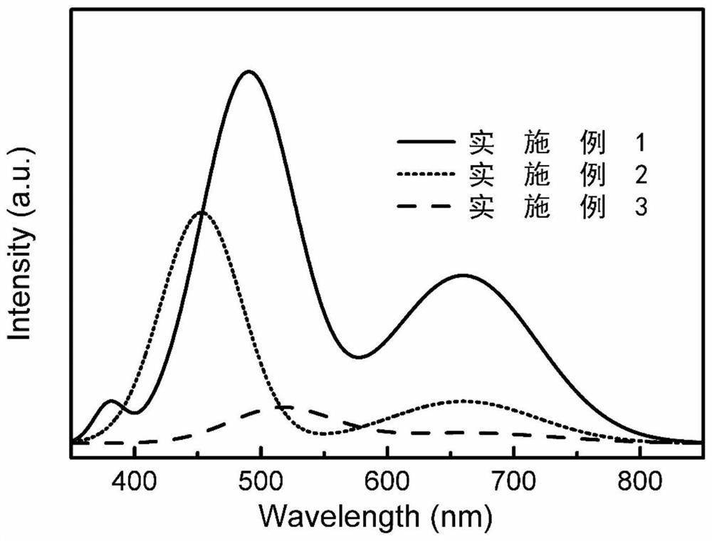
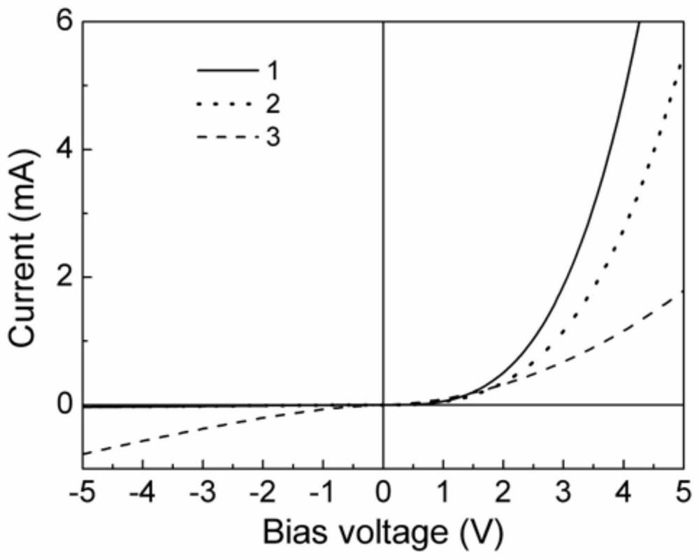
[0039] The preparation method is the same as in Example 1, but step 2 is omitted, and the prepared device is a PMOT:PPV / ZnO:Al heterojunction. From figure 1 It can be seen that the main luminescence peak changes from around 490nm to around 450nm after shifting, indicating that it cannot have the same photobiological enhancement effect as Example 1, and its luminous intensity is obviously weaker than that of Example 1. From figure 2 It can be seen that the forward current is small, the reverse current is large, the rectification ratio is low, the rectification effect of the current-voltage characteristics is not as good as that of Example 1, and the electric injection efficiency is not as good as that of Example 1, because the device energy band structure of Example 2 Not as reasonable as that made in Example 1.
Embodiment 3
[0040] Embodiment 3 (contrast):
[0041] The preparation method and test are the same as in Example 1, but step 4 is omitted. From figure 1 It can be seen that the main peak of the photobiological effect at 490nm is significantly weaker than that of Example 1, and the overall luminous intensity is also significantly weaker than that of Example 1. From figure 2 It can be seen that the forward current is small, the reverse current is large, the rectification ratio is low, the rectification effect of the current-voltage characteristics is not as good as that of Example 1, and the electric injection efficiency is not as good as that of Example 1, because Example 3 has not been treated with plasma. The surface impurities of the PMOT:PPV / ZnO:Cu / ZnO:Al heterojunction LED are more than the surface impurities of the PMOT:PPV / ZnO:Cu / ZnO:Al heterojunction LED treated by plasma in Example 1.
PUM
 Abstract
Description
Claims
Application Information
 - R&D
- Intellectual Property
- Life Sciences
- Materials
- Tech Scout
- Unparalleled Data Quality
- Higher Quality Content
- 60% Fewer Hallucinations
Browse by: Latest US Patents, China's latest patents, Technical Efficacy Thesaurus, Application Domain, Technology Topic, Popular Technical Reports.
© 2025 PatSnap. All rights reserved.Legal|Privacy policy|Modern Slavery Act Transparency Statement|Sitemap|About US| Contact US: help@patsnap.com


