Display substrate, manufacturing method thereof and display device

A display substrate and manufacturing method technology, applied in semiconductor/solid-state device manufacturing, electrical components, electrical solid-state devices, etc., can solve problems such as poor lap joints, affecting product yield, and output electrodes are easily over-etched, achieving Good lap performance and the effect of improving product yield

Active Publication Date: 2020-02-07
BOE TECH GRP CO LTD +1
View PDF4 Cites 3 Cited by
  • Summary
  • Abstract
  • Description
  • Claims
  • Application Information

AI Technical Summary

Problems solved by technology

[0005] The purpose of the present invention is to provide a display substrate and its manufacturing method, and a display device, which are used to solve the problem of simultaneously etching the flat layer to form via holes for exposing the output electrodes and exposing the compensation under the same etching conditions. When the via hole of the cathode pattern is used, the output electrode is easily over-etched, resulting in poor subsequent lap connection with the anode, which affects the product yield.

Method used


Image

  • Display substrate, manufacturing method thereof and display device
  • Display substrate, manufacturing method thereof and display device
  • Display substrate, manufacturing method thereof and display device

Examples


Embodiment Construction

[0059] In order to further illustrate the display substrate, the manufacturing method thereof, and the display device provided by the embodiments of the present invention, a detailed description will be given below in conjunction with the accompanying drawings.

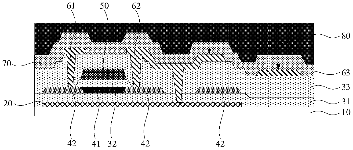
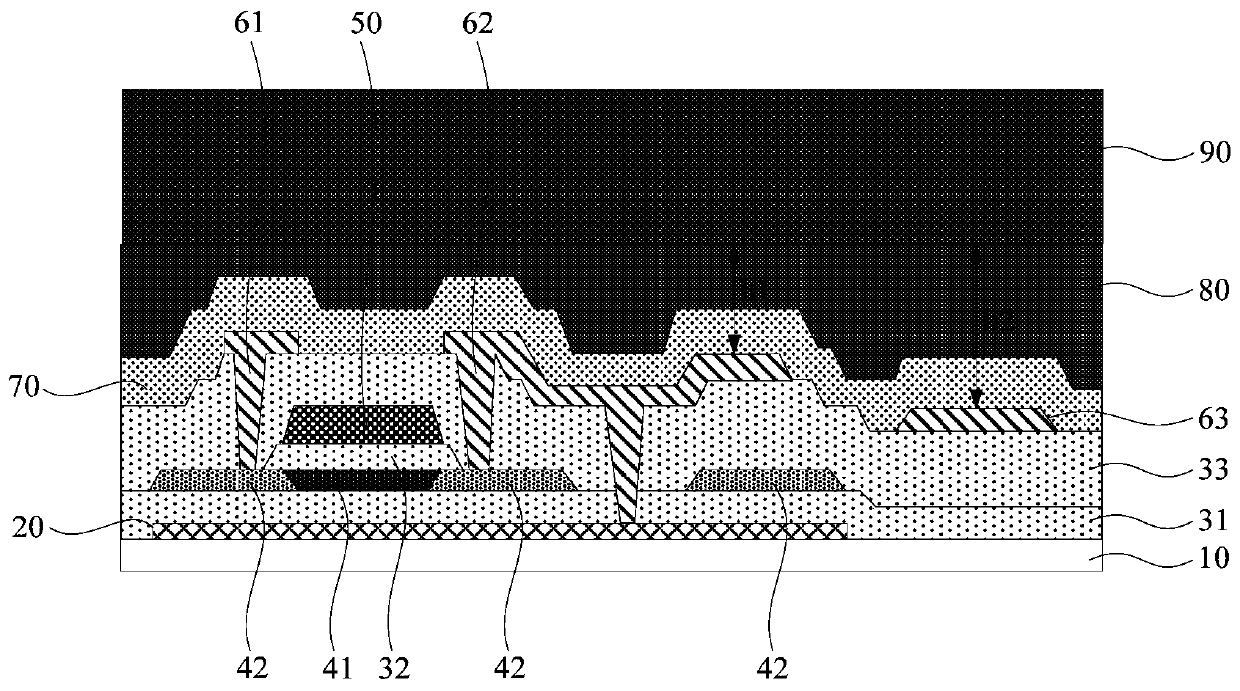
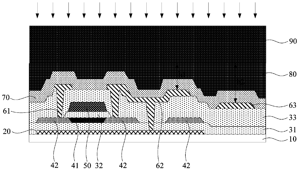
[0060] Taking OLED display substrates with top emission structure as an example, such as figure 1 with Figure 2f As shown, the first transistor for outputting the driving signal includes: a semiconductor active layer 41, a conductive connection structure 42 located on both sides of the semiconductor active layer 41 and coupled with the semiconductor active layer 41, and a gate insulating layer 32 , the gate 50, the first insulating layer 33, the input electrode 61 and the output electrode 62. A light-shielding layer 20 and a conductive connection structure 42 are arranged between the output electrode 62 of the first transistor and the substrate 10, so that in the direction perpendicular to the substrate 10, the outp...


PUM


Abstract

The invention provides a display substrate, a manufacturing method thereof and a display device, which relate to the technical field of display and solve the problem that when a flat layer is etched at the same time to form a via hole exposing an output electrode and a via hole exposing a compensation cathode pattern, the output electrode is easily over-etched, and subsequent poor lap joint with an anode is caused. The manufacturing method comprises steps: a photoresist layer is exposed, the orthographic projection of a formed photoresist half-reserved area on the substrate is located in the orthographic projection of an output electrode on the substrate, and the orthographic projection of a photoresist complete removal area on the substrate is located in the orthographic projection of a compensation cathode pattern on the substrate; and the photoresist located in the photoresist half-reserved area, a flat layer corresponding to the photoresist half-reserved area and the flat layer corresponding to the photoresist complete removal area are etched, and a first via hole exposing the surface, back to the substrate, of the output electrode and a second via hole exposing the surface, back to the substrate, of the compensation cathode pattern are formed at the same time. The manufacturing method provided by the invention is used for manufacturing the display substrate.

Description

technical field [0001] The invention relates to the field of display technology, in particular to a display substrate, a manufacturing method thereof, and a display device. Background technique [0002] When making a large-sized organic light-emitting diode (English: Organic Light-Emitting Diode, referred to as OLED) display substrate, generally a compensation cathode pattern is provided in the display substrate, and the compensation cathode pattern is coupled to the cathode in the OLED display substrate , to reduce the resistance of the cathode. The display substrate also includes a transistor for outputting a driving signal, and a light-shielding layer and a conductive functional pattern are generally arranged directly under the output electrode of the transistor, so that in a direction perpendicular to the base of the display substrate, the output electrode faces away from the base The height of the surface is higher than the height of the surface of the compensation cat...

Claims


Application Information

Patent Timeline
Patent Type & Authority Applications(China)
IPC IPC(8): H01L21/027H01L27/32
CPCH01L21/0274H10K59/88H10K59/00H10K59/12
Inventor 宋威赵策王明丁远奎刘宁刘军李伟王庆贺
Owner BOE TECH GRP CO LTD
Why Eureka
Try Eureka